Yaskawa Ladder Works Programming Manual User Manual
Page 137
7.6 PID CONTROL Instruction (PID)
7-16
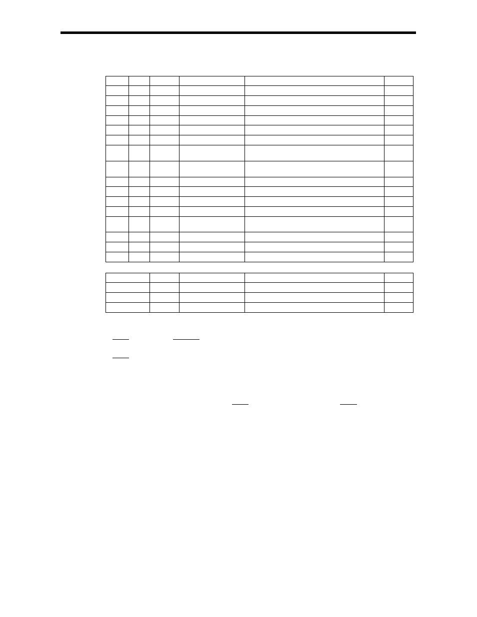
Table of Real Type PID Instruction Parameters
ADR
Type Symbol
Name
Specification
I/O
0
W
RLY
Relay I/O
Relay input, relay output *
1
IN/OUT
1 W -
(Reserve) Reserve
register
-
2
F
Kp
P gain
Gain of the P correction
IN
4
F
Ki
I gain
Gain of the integration circuit
IN
6
F
Kd
D gain
Gain of the differentiation circuit input
IN
8
F
Ti
Integration time
Integration time (s)
IN
10 F
Td1 Divergence
differentiation time
The differentiation time (s) used in the case of
diverging input.
IN
12 F
Td2 Convergence
differentiation time
The differentiation time (s) used in the case of
converging input.
IN
14
F
IUL
Upper integration limit
Upper limit for the I correction value
IN
16
F
ILL
Lower integration limit
Lower limit for the I correction value
IN
18
F
UL
Upper PID limit
Upper limit for the P+I+D correction value
IN
20
F
LL
Lower PID limit
Lower limit for the P+I+D correction value
IN
22
F
DB
PID output dead band
Width of the dead band for the P+I+D correction
value
IN
24
F
Y
PID output
PID correction output (also output to the A register)
OUT
26
F
Ti
I correction value
Storage of the I correction value
OUT
28
F
X
Input value storage
Storage of the present deviation input value
OUT
*
1
:Relay I/O Bit Assignment
BIT
Symbol
Name
Specification
I/O
0
IRST
Integration reset
"ON" is input when integration is reset.
IN
1 to 7
-
(Reserve)
Reserve relay for input
IN
8 to F
-
(Reserve)
Reserve relay for output
OUT
Here, the PID operation is expressed as follows:
Y 1
X
Kp + Ki×
Ti×S
= Kd×Td×S
Y
X
= Kp+Kd×Td×S
X : deviation input value
Y : output value
The following opertion is performed within the PID instruction:
Ti Td
Y = Kp×X +{ ( Ki×X + IREM ) /
Ts
+ Yi'}+ Kd× ( X – X' )×
Ts
X' : previous input value
Yi' : previous I output value
Ts : scan time set value