I/o and clocking resources, I/o and clocking resources –5 – Altera Cyclone III Development Board User Manual
Page 15
Chapter 2: Board Components
2–5
Featured FPGA (U20)
© March 2009 Altera Corporation
Cyclone III 3C120 Development Board Reference Manual
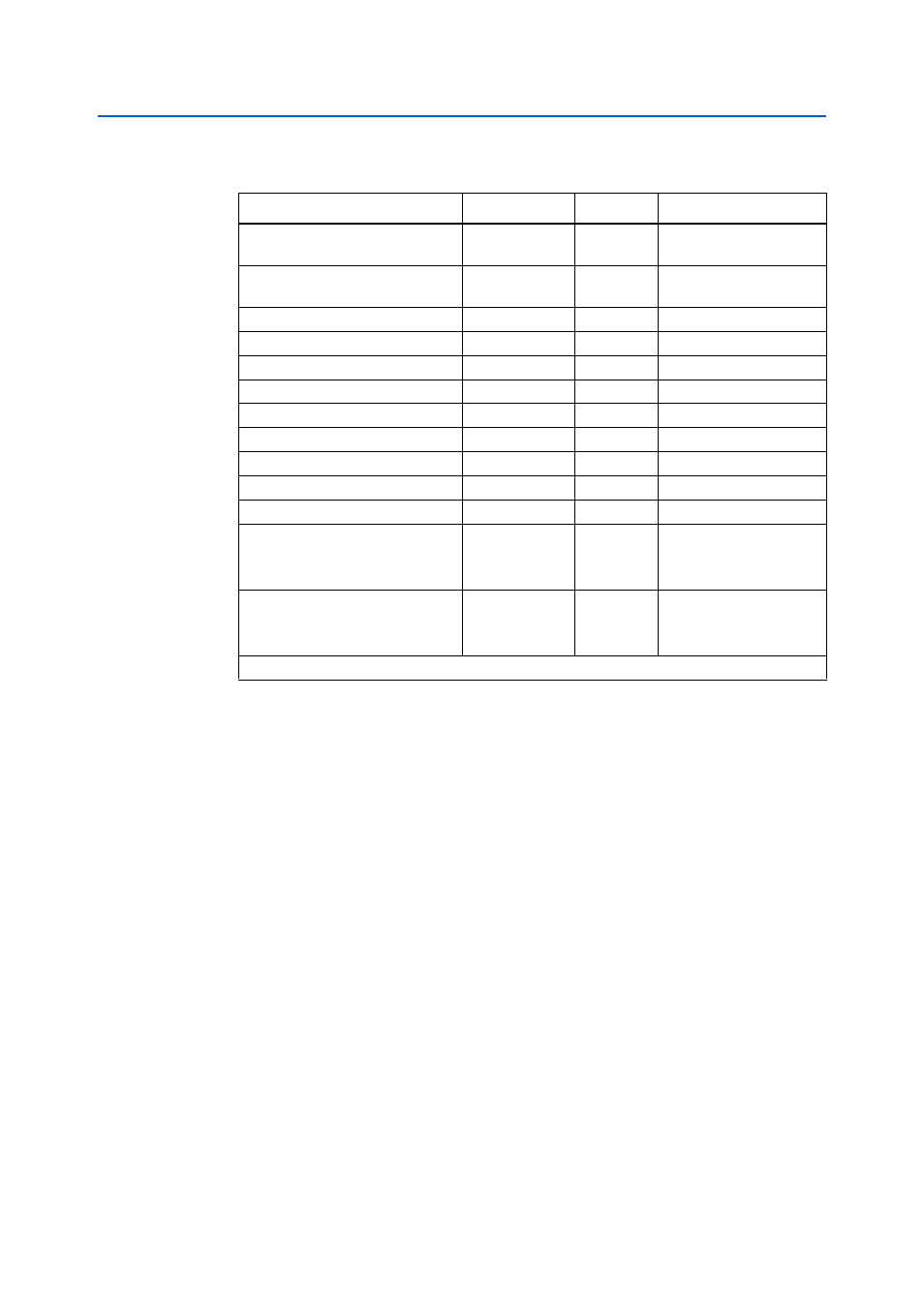
lists the Cyclone III EP3C120F780C7 device pin count.
f
For additional information about Altera devices, go to
I/O and Clocking Resources
This section lists specific I/O and clocking resources available with the
EP3C120F780C7 device, which is the largest of the Cyclone III devices.
illustrates the available I/O bank resources on the EP3C120F780C7 device.
Table 2–4. Cyclone III Device Pin Count
Function
I/O Type
I/O Count
Special Pins
Oscillators and SMAs
1.8-V CMOS
4
Three clock inputs, one
output
DDR2
1.8-V SSTL
148
Nine data strobe signal
(DQS), 10 V
REF
Flash/SRAM/MAX
1.8-V CMOS
78
—
Horizontal bank OCT calibration
1.8-V CMOS
4
2 Rup, 2 Rdn
Vertical bank OCT calibration
2.5-V CMOS
4
2 Rup, 2 Rdn
Passive serial configuration
2.5-V CMOS
2
DATAO
, DCLK
Ethernet
2.5-V CMOS
16
1 clock input
Buttons, Switches, LEDs
1.8-V CMOS
34
DEV_CLR
Character LCD, Graphics LCD
2.5-V CMOS
14
—
Speaker header
2.5-V CMOS
1
—
USB
2.5-V CMOS
14
1 clock input
HSMC Port A
2.5-V CMOS
2.5-V LVDS
86
5 clock inputs
(1 single-ended,
2 differential)
HSMC Port B
2.5-V CMOS
2.5-V LVDS
86
5 clock inputs
(1 single-ended,
2 differential)
Device I/O total: 491