Block diagram, Block diagram –4, Power supply – Altera Cyclone III Development Board User Manual
Page 8: 14 v – 20 v dc input, On-board power measurement circuitry, Up to 19.8 w per hsmc interface, Mechanical, 6” × 8” board
1–4
Chapter 1: Overview
General Description
Cyclone III 3C120 Development Board Reference Manual
© March 2009 Altera Corporation
■
Power supply
■
14 V – 20 V DC input
■
On-board power measurement circuitry
■
Up to 19.8 W per HSMC interface
■
Mechanical
■
6” × 8” board
■
Bench-top design
1
The Cyclone III FPGA Development Kit ships with additional HSMC daughter card
loopback and break-out headers for convenient testing of some of the HSMC signals.
For more details regarding these test daughter cards, refer to their respective
schematics at these locations in the installed kit directory:
■
<path>\board_design_files\schematic\breakout_hsmc
debug_header_breakout.pdf
■
<path>\board_design_files\schematic\loopback_hsmc
loopback_test_lowcost.pdf
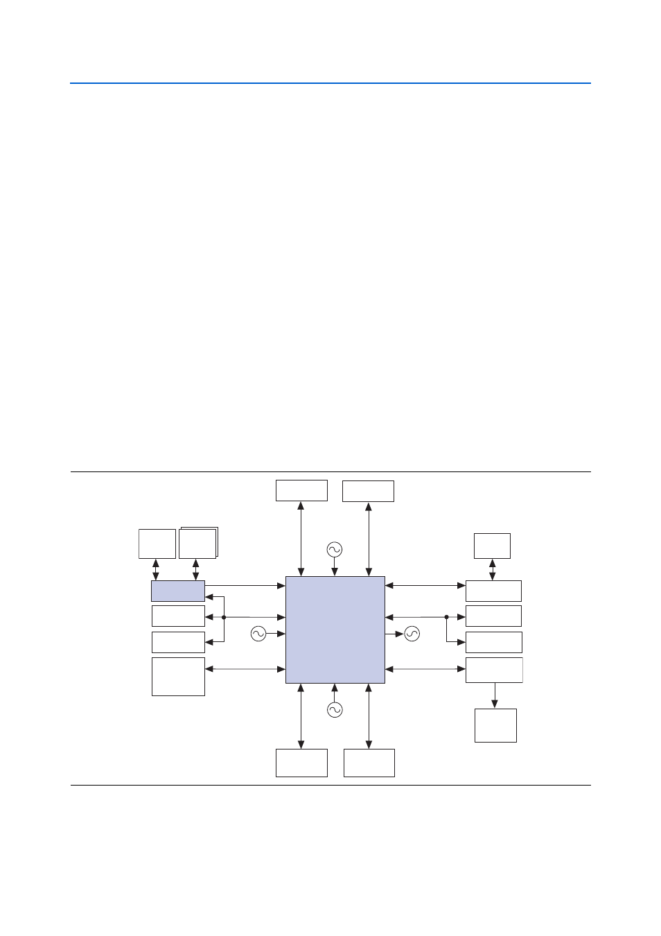
Block Diagram
shows the functional block diagram of the Cyclone III development board.
Figure 1–1. Cyclone III Development Board Block Diagram
CMOS + LVDS
Cyclone III
EP3C120F780
125 MHz
XTAL
SMA Input
MAX II
Device (x32)
2.5V CMOS
1.8V CMOS
Power
Measure/
Display
HSMC Port A
CMOS + LVDS
HSMC Port B
8MB SRAM
(x32)
64MB Flash
(x16)
256MB DDR2
Dual Channel
(x72)
USB
2.0
1.8V CMOS
50 MHz
Buttons/
Switches
1.8V CMOS
Quad 7-Seg/
User LEDs
1.8V SSTL
SMA Output
10/100/1000
Ethernet
2.5V CMOS
2.5V CMOS
RJ-45
Jack
Graphics LCD
Character LCD
LP Filter and
Audio Amp
2.5V CMOS
PC
Speaker
Header