Altera Cyclone III Development Board User Manual
Page 66
2–56
Chapter 2: Board Components
On-Board Memory
Cyclone III 3C120 Development Board Reference Manual
© March 2009 Altera Corporation
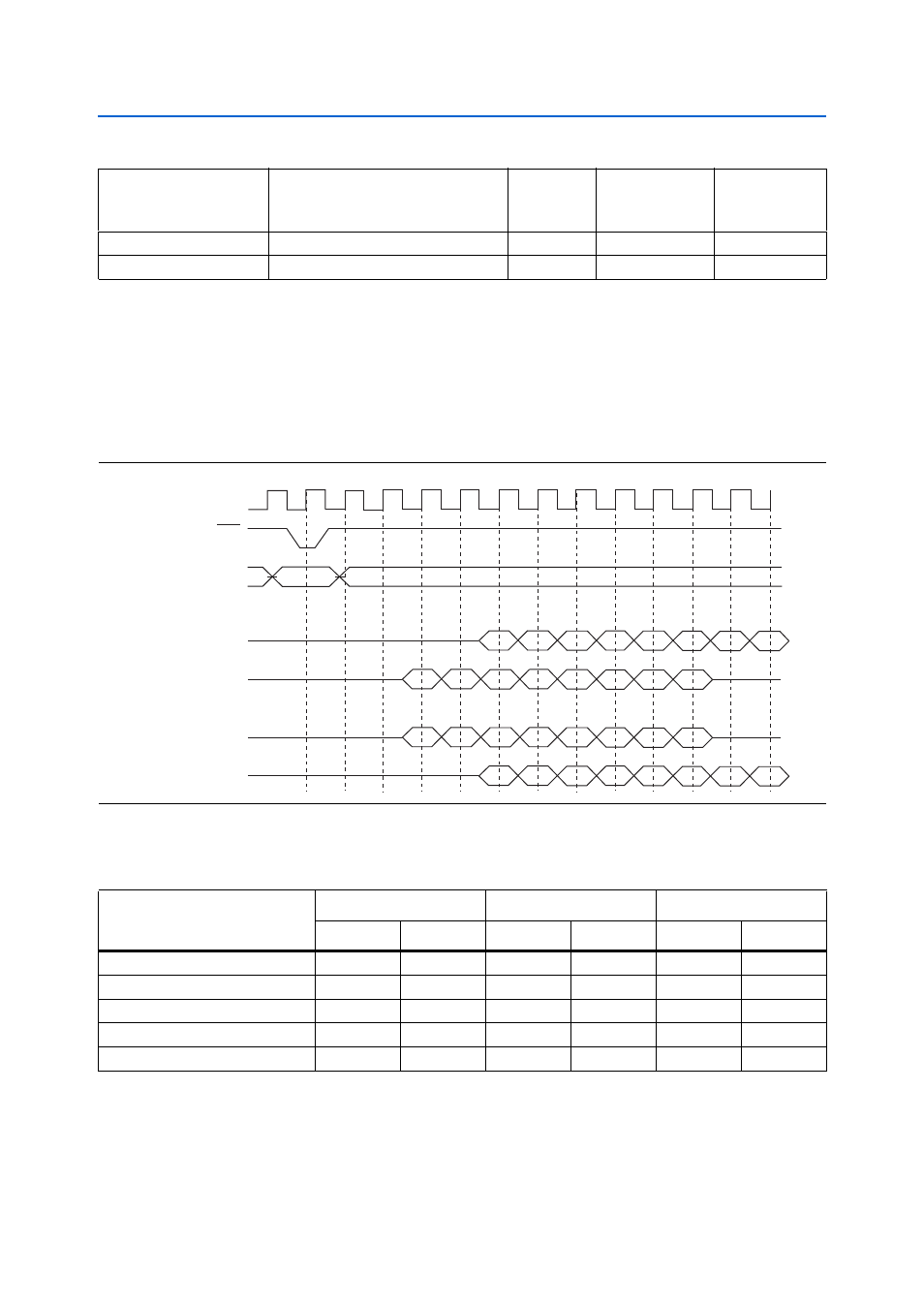
illustrates the latency for both fixed and variable modes of operation. For
asynchronous accesses, each of the two devices has its own WAIT pin wired to the
Cyclone III device.
f
For Samsung SRAM pin definitions, data sheet, and other related documentation,
refer to the Samsung website at
.
lists the Samsung device latency values based on operation frequency.
U24 pin F1
Data bit 30
1.8 V
FSD30
H10
U24 pin G1
Data bit 31
1.8 V
FSD31
J10
Table 2–53. SRAM Interface I/O (Part 3 of 3)
Board
Reference
Description
I/O Standard
Schematic Signal
Name
Cyclone III
Device Pin
Number
Figure 2–14. SRAM Latency Timing Illustration
1st
Clock
Address
Data Out
Data In
Data In/Out
Data Out
Latency 4 (Burst Length: 8)
Fixed Latency - A18[0]
Variable Latency - A18[1]
Latency 2 (Burst Length: 8)
2nd
3rd
4th
5th
D0
D1
D2
6th
7th
8th
9th
10th
11th
D3
D4
D5
D6
D7
D0
D1
D2
D3
D4
D5
D6
D7
Q0
Q1
Q2
Q3
Q4
Q5
Q6
Q7
DQ0
DQ1
DQ2
DQ3
DQ4
DQ5
DQ6
DQ7
ADV
Latency 4 (Burst Length: 8)
Latency 2 (Burst Length: 8)
Table 2–54. SRAM Latency Vs. Frequency
Item
Up to 66 MHz
Up to 80 MHz
Up to 104 MHz
Fixed
Variable
Fixed
Variable
Fixed Variable
Latency set (A11:A10:A9)
4(0:0:1)
2(1:0:0)
5(0:1:0)
3(0:0:0)
7(1:0:1)
4(0:0:1)
Read latency (min)
4
2/4
5
3/5th
7
4/7
First read data fetch clock
5th
3rd/5th
6th
4th/6th
8th
5th/8th
Write latency (min)
2
2
3
3
4
4
First write data loading clock
3rd
3rd
3rd
4th
5th
5th