Altera Cyclone III Development Board User Manual
Page 55
Chapter 2: Board Components
2–45
Communication Ports and Interfaces
© March 2009 Altera Corporation
Cyclone III 3C120 Development Board Reference Manual
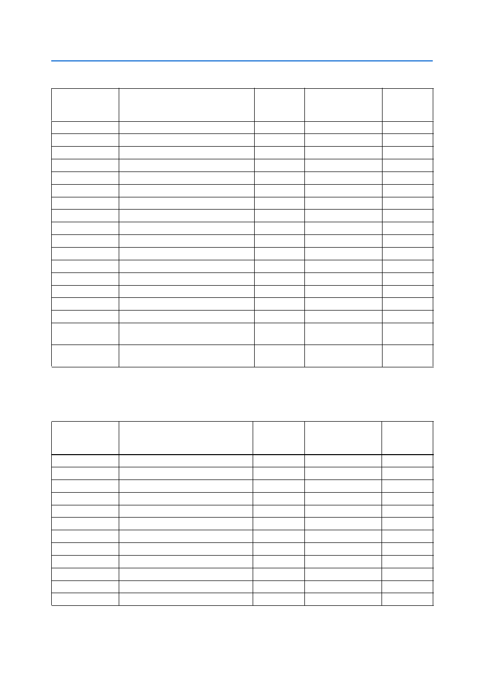
lists the HSMC Port B interface signal name, description, and I/O
standard. Signal name and direction are relative to the Cyclone III FPGA, which is the
HSMC host.
J8 pin 137
LVDS TX 14p or CMOS I/O data bit 64
LVDS or 2.5 V
HSMA_TX_D_P14
F5
J8 pin 138
LVDS TX 14p or CMOS I/O data bit 65
LVDS or 2.5 V
HSMA_RX_D_P14
G4
J8 pin 139
LVDS RX 14n or CMOS I/O data bit 66
LVDS or 2.5 V
HSMA_TX_D_N14
F4
J8 pin 140
LVDS RX 14n or CMOS I/O data bit 67
LVDS or 2.5 V
HSMA_RX_D_N14
G3
J8 pin 143
LVDS RX 15p or CMOS I/O data bit 68
LVDS or 2.5 V
HSMA_TX_D_P15
E2
J8 pin 144
LVDS TX 15p or CMOS I/O data bit 69
LVDS or 2.5 V
HSMA_RX_D_P15
F2
J8 pin 145
LVDS RX 15n or CMOS I/O data bit 70
LVDS or 2.5 V
HSMA_TX_D_N15
E1
J8 pin 146
LVDS TX 15n or CMOS I/O data bit 71
LVDS or 2.5 V
HSMA_RX_D_N15
F1
J8 pin 149
LVDS RX 16p or CMOS I/O data bit 72
LVDS or 2.5 V
HSMA_TX_D_P16
D3
J8 pin 150
LVDS TX 16p or CMOS I/O data bit 73
LVDS or 2.5 V
HSMA_RX_D_P16
E3
J8 pin 151
LVDS TX 16n or CMOS I/O data bit 74
LVDS or 2.5 V
HSMA_TX_D_N16
C2
J8 pin 152
LVDS RX 16n or CMOS I/O data bit 75
LVDS or 2.5 V
HSMA_RX_D_N16
F3
J8 pin 155
LVDS or CMOS clock out
LVDS
HSMA_CLK_OUT_P2
D2
J8 pin 156
LVDS or CMOS clock in
LVDS
HSMA_CLK_IN_P2
J2
J8 pin 157
LVDS or CMOS clock out
2.5 V
HSMA_CLK_OUT_N2
D1
J8 pin 158
LVDS or CMOS clock in
2.5 V
HSMA_CLK_IN_N2
J1
N/A
User LED intended to show RX data
activity on the HSMC interface
2.5 V
HSMA_RX_LED
AE1
N/A
User LED intended to show TX data
activity on the HSMC interface
2.5 V
HSMA_TX_LED
AA3
Table 2–47. HSMC Port A Interface Signal Name, Description, and Type (Part 3 of 3)
Board
Reference
Description
I/O Standard
Schematic
Signal Name
Cyclone III
Device Pin
Number
Table 2–48. HSMC Port B Interface Signal Name, Description, and Type (Part 1 of 4)
Board
Reference
Description
I/O Standard
Schematic
Signal Name
Cyclone III
Device Pin
Number
J9 pin 33
Management serial data
2.5 V
HSMB_SDA
H26
J9 pin 34
Management serial clock
2.5 V
HSMB_SCL
H25
J9 pin 35
JTAG clock signal
2.5 V
FPGA_JTAG_TCK
P5
J9 pin 36
JTAG mode select signal
2.5 V
FPGA_JTAG_TMS
P8
J9 pin 39
Dedicated CMOS clock out
2.5 V
HSMB_CLK_OUT0
J22
J9 pin 40
Dedicated CMOS clock in
2.5 V
HSMB_CLK_IN0
A15
J9 pin 41
Dedicated CMOS I/O bit 0
2.5 V
HSMB_D0
G24
J9 pin 42
Dedicated CMOS I/O bit 1
2.5 V
HSMB_D1
H23
J9 pin 43
Dedicated CMOS I/O bit 2
2.5 V
HSMB_D2
G25
J9 pin 44
Dedicated CMOS I/O bit 3
2.5 V
HSMB_D3
H24
J9 pin 47
LVDS TX 0p or CMOS I/O data bit 4
LVDS or 2.5 V
HSMB_TX_D_P0
J25
J9 pin 48
LVDS RX 0p or CMOS I/O data bit 5
LVDS or 2.5 V
HSMB_RX_D_P0
F27