Sram, Sram –54 – Altera Cyclone III Development Board User Manual
Page 64
2–54
Chapter 2: Board Components
On-Board Memory
Cyclone III 3C120 Development Board Reference Manual
© March 2009 Altera Corporation
SRAM
The board features 8 MB of SRAM memory with a 32-bit data bus. The devices use
1.8-V CMOS signaling and are optimized for low cost and power.
The 32-bit interface comprises two ×16 devices. The Samsung part features a
maximum frequency of 104 MHz (104 Mbps). The theoretical bandwidth of the entire
interface is 416 Mbps.
The SRAM devices are part of a shared bus with connectivity to the MAX II CPLD as
well as the flash memory, which is called the FSM bus. All three devices use 1.8-V
CMOS signaling. Altera recommends using the 50-
Ω OCT setting on the FPGA and
the one-half drive setting on the SRAM.
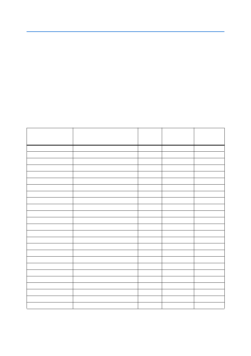
lists the SRAM interface signal name, description, and I/O standard.
Signal name and type are relative to the Cyclone III device, i.e., I/O setting and
direction.
Table 2–53. SRAM Interface I/O (Part 1 of 3)
Board
Reference
Description
I/O Standard
Schematic Signal
Name
Cyclone III
Device Pin
Number
U23 pin A1
Byte enables bit 0
1.8 V
SRAM_BEn0
AF20
U23 pin B2
Byte enables bit 1
1.8 V
SRAM_BEn1
AH26
U24 pin A1
Byte enables bit 2
1.8 V
SRAM_BEn2
AE22
U24 pin B2
Byte enables bit 3
1.8 V
SRAM_BEn3
AB21
U23, U24 pin J2
Clock (drives two memories)
1.8 V
SRAM_CLK
AD22
U23, U24 pin B5
Chip select
1.8 V
SRAM_CSn
AB19
U23, U24 pin A2
Output enable
1.8 V
SRAM_OEn
AD25
U23, U24 pin A6
Power save /MRS set pin
1.8 V
SRAM_PSn
B4
U23 pin J1
Data wait bit 0
1.8 V
SRAM_WAIT0
AG15
U24 pin J1
Data wait bit 1
1.8 V
SRAM_WAIT1
AH25
U23, U24 pin G5
Write enable
1.8 V
SRAM_WEn
AE25
U23, U24 pin J3
Address valid
1.8 V
SRAM_ADVn
AA19
U23, U24 pin A3
Address bit 1 (DWORD aligned)
1.8 V
FSA1
AH10
U23, U24 pin A4
Address bit 2 (DWORD aligned)
1.8 V
FSA2
AA13
U23, U24 pin A5
Address bit 3 (DWORD aligned)
1.8 V
FSA3
AC10
U23, U24 pin B3
Address bit 4 (DWORD aligned)
1.8 V
FSA4
Y15
U23, U24 pin B4
Address bit 5 (DWORD aligned)
1.8 V
FSA5
AF22
U23, U24 pin C3
Address bit 6 (DWORD aligned)
1.8 V
FSA6
AF26
U23, U24 pin C4
Address bit 7 (DWORD aligned)
1.8 V
FSA7
AF4
U23, U24 pin D4
Address bit 8 (DWORD aligned)
1.8 V
FSA8
AD8
U23, U24 pin H2
Address bit 9 (DWORD aligned)
1.8 V
FSA9
AG26
U23, U24 pin H3
Address bit 10 (DWORD aligned)
1.8 V
FSA10
AH6
U23, U24 pin H4
Address bit 11 (DWORD aligned)
1.8 V
FSA11
AD24
U23, U24 pin H5
Address bit 12 (DWORD aligned)
1.8 V
FSA12
AF9
U23, U24 pin G3
Address bit 13 (DWORD aligned)
1.8 V
FSA13
AA8