Power select rotary switch –21, Table 2–14 – Altera Cyclone III Development Board User Manual
Page 31
Chapter 2: Board Components
2–21
Configuration, Status, and Setup Elements
© March 2009 Altera Corporation
Cyclone III 3C120 Development Board Reference Manual
lists the push-button switch component reference and manufacturing
information.
f
For information about user-defined push buttons, refer to
POWER SELECT Rotary Switch
A 16-position rotary switch, board reference SW4, is used to select the current power
rail whose power is being measured and displayed on the power display. The rotary
switch is connected to the MAX II CPLD, but it also registers readable by the FPGA
using the FSM shared bus (flash, SRAM, and MAX II device).
lists the
power select rotary switch number, name, power pin, and description.
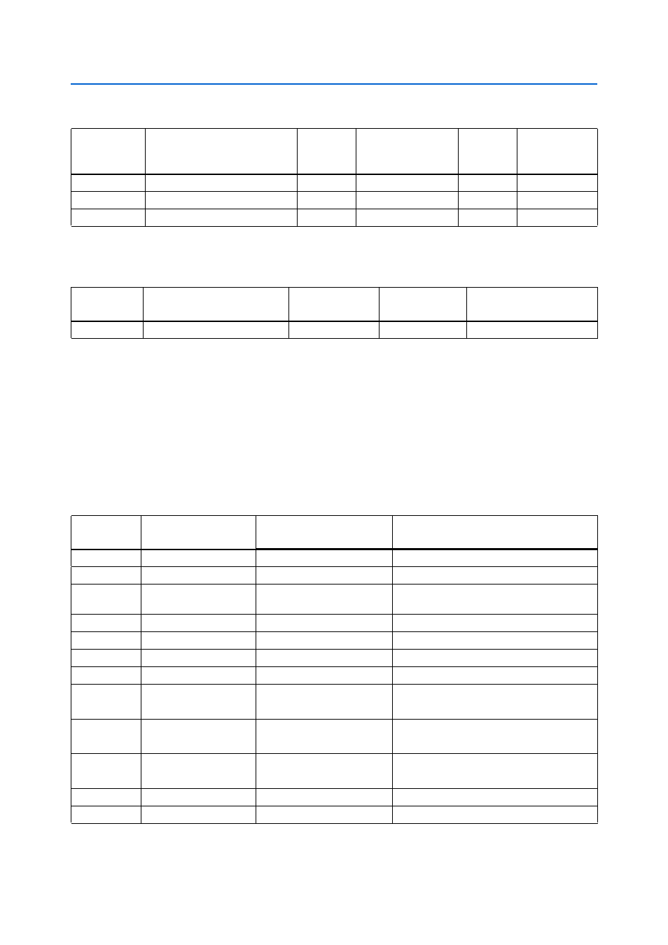
Table 2–14. Push Button Switch Signal Name and Function
Board
Reference
Description
I/O
Standard
Schematic
Signal Name
Cyclone III
Device
Pin Number
MAX II
Device
Pin Number
S7
User defined push button
1.8 V
FACTORY_CONFIG
—
A10
S6
User defined push button
1.8 V
RESET_CONFIGn
—
R16
S5
User defined push button
1.8 V
CPU_RESET
T21
M9
Table 2–15. Push-Button Switch Component Reference and Manufacturing Information
Board
Reference
Description
Manufacturer
Manufacturing
Part Number
Manufacturer
Website
S5-S7
Push button switch
Panasonic
EVQAPAC07K
Table 2–16. Power Select Rotary Switch Number, Name, Pin, and Description (Part 1 of 2)
Number
Schematic
Signal Name
Power Pin Name
Description
0
1.2V_INT
VCCINT
FPGA core power
1
1.2V_VCCD
VCCD_PLL
FPGA PLL digital power
2
2.5V_VCCA
VCCA
FPGA PLL analog power and auxiliary circuit
power
3
1.8V_IO_B3_B4
VCCIO3
, VCCIO4
FPGA I/O power banks 3, 4
4
1.8V_IO_B7_B8
VCCIO7
, VCCIO8
FPGA I/O power banks 7, 8
5
2.5V_IO_B1_B2
VCCIO1
, VCCIO2
FPGA I/O power banks 1, 2
6
2.5V_IO_B5_B6
VCCIO5
, VCCIO6
FPGA I/O power banks 5, 6
7
1.2V
—
All non-FPGA 1.2-V power
(Ethernet)
8
1.8V
—
All non-FPGA 1.8-V power
(SRAM, Flash, MAX II, and DDR2 devices)
9
2.5V
—
All non-FPGA 2.5-V power
(Ethernet, LEDs, LCD)
A
3.3V
—
All 3.3-V power (voltage only)
B
5.0V
—