Altera Cyclone III Development Board User Manual
Page 59
Chapter 2: Board Components
2–49
On-Board Memory
© March 2009 Altera Corporation
Cyclone III 3C120 Development Board Reference Manual
The two address buses are large enough to support any size JEDEC-compliant DDR2
device, as they have all 16 address pins and all three bank pins connected. The Micron
components shipped on the board all have 13 row addresses, 2 bank addresses, and
10 column addresses.
1
Unused control pins should be left tri-stated to reduce power consumption.
There are three clock pairs driven from the FPGA to the memories. The first two pairs
clock two memory devices each. The last clock drives the 5th memory device as well
as an additional capacitive load to make all clocks have similar loading.
The maximum frequency is 167 MHz (333 Mbps per pin). The theoretical bandwidth
of the entire DDR2 interface is 2667 Mbps plus ECC, or 3,000 Mbps raw throughput.
f
For more information, visit Micron at
The data interface to the FPGA fabric runs at either one-half or one-quarter the
physical layer data rate when using the Altera DDR2 MegaCore function, which
equates to a doubling or quadrupling of the physical data bus width (144 bits or
288 bits, respectively). For example, a 72-bit interface with a 200-MHz external clock
speed can have a 200 MHz 144-bit internal bus or a 100 MHz 288-bit interface.
To allow for the use of memory device ODT functionality, the ODT signal is
connected. Because a board-level Class I termination is also available, use of this
feature is optional. Termination resistors are approximately 50
Ω to match the trace
impedance of the signals on the board. Clocks are terminated using a single 100
Ω
resistor across each P/N pair. Altera recommends using the 50
Ω OCT on the FPGA
for data, and the 10 mA setting for the address and control pins. The DDR2 devices
should use the reduced drive strength setting available as a register option.
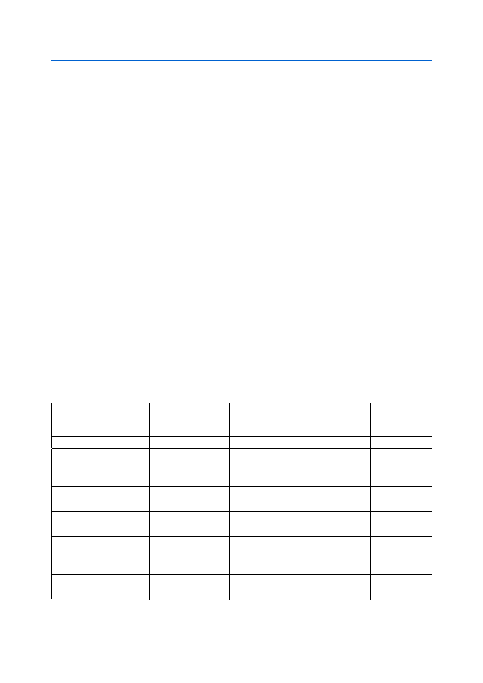
lists the DDR2 interface signal name, description, and I/O standard. Signal
name and direction are relative to the Cyclone III FPGA.
Table 2–51. DDR2 Interface I/O (Part 1 of 5)
Board
Reference
Description
I/O Standard
Schematic
Signal Name
Cyclone III
Device Pin
Number
U25, U26 pin K8
Differential clock 0n
SSTL18 Class 1
DDR2_CK_N0
AF14
U11, U12 pin K8
Differential clock 1n
SSTL18 Class 1
DDR2_CK_N1
G11
U13 pin F8
Differential clock 2n
SSTL18 Class 1
DDR2_CK_N2
H19
U25, U26 pin J8
Differential clock 0p
SSTL18 Class 1
DDR2_CK_P0
AE14
U11, U12 pin J8
Differential clock 1p
SSTL18 Class 1
DDR2_CK_P1
H12
U13 pin E8
Differential clock 2p
SSTL18 Class 1
DDR2_CK_P2
J19
U26 pin F3
Data mask 0
SSTL18 Class 1
DDR2_DM0
AH19
U26 pin B3
Data mask 1
SSTL18 Class 1
DDR2_DM1
AC15
U25 pin F3
Data mask 2
SSTL18 Class 1
DDR2_DM2
AF8
U25 pin B3
Data mask 3
SSTL18 Class 1
DDR2_DM3
AB9
U11 pin F3
Data mask 4
SSTL18 Class 1
DDR2_DM4
B10
U11 pin B3
Data mask 5
SSTL18 Class 1
DDR2_DM5
A8
U12 pin F3
Data mask 6
SSTL18 Class 1
DDR2_DM6
E15