Character lcd (j4) –32 – Altera Cyclone III Development Board User Manual
Page 42
2–32
Chapter 2: Board Components
General User Interfaces
Cyclone III 3C120 Development Board Reference Manual
© March 2009 Altera Corporation
Character LCD (J4)
The board contains a single 14-pin 0.1” pitch dual-row header, used to interface to a
16-character by 2-line LCD display, Lumex (part number LCM-S01602DSR/C). The
LCD has a 14-pin receptacle that mounts directly to the board’s 14-pin header, so it
can be easily removed for access to components under the display—or to use the
header for debugging or other purposes.
summarizes the character LCD interface pins. Signal name and direction
are relative to the Cyclone III FPGA. For functional descriptions, see
shows pin definitions, and is an excerpt from the Lumex data sheet.
f
For more information such as timing, character maps, interface guidelines, and
related documentation, visit
.
shows a functional block diagram of the Lumex LCD display device. The
8-bit data bus is shared with the graphics LCD, but the control signals are all separate.
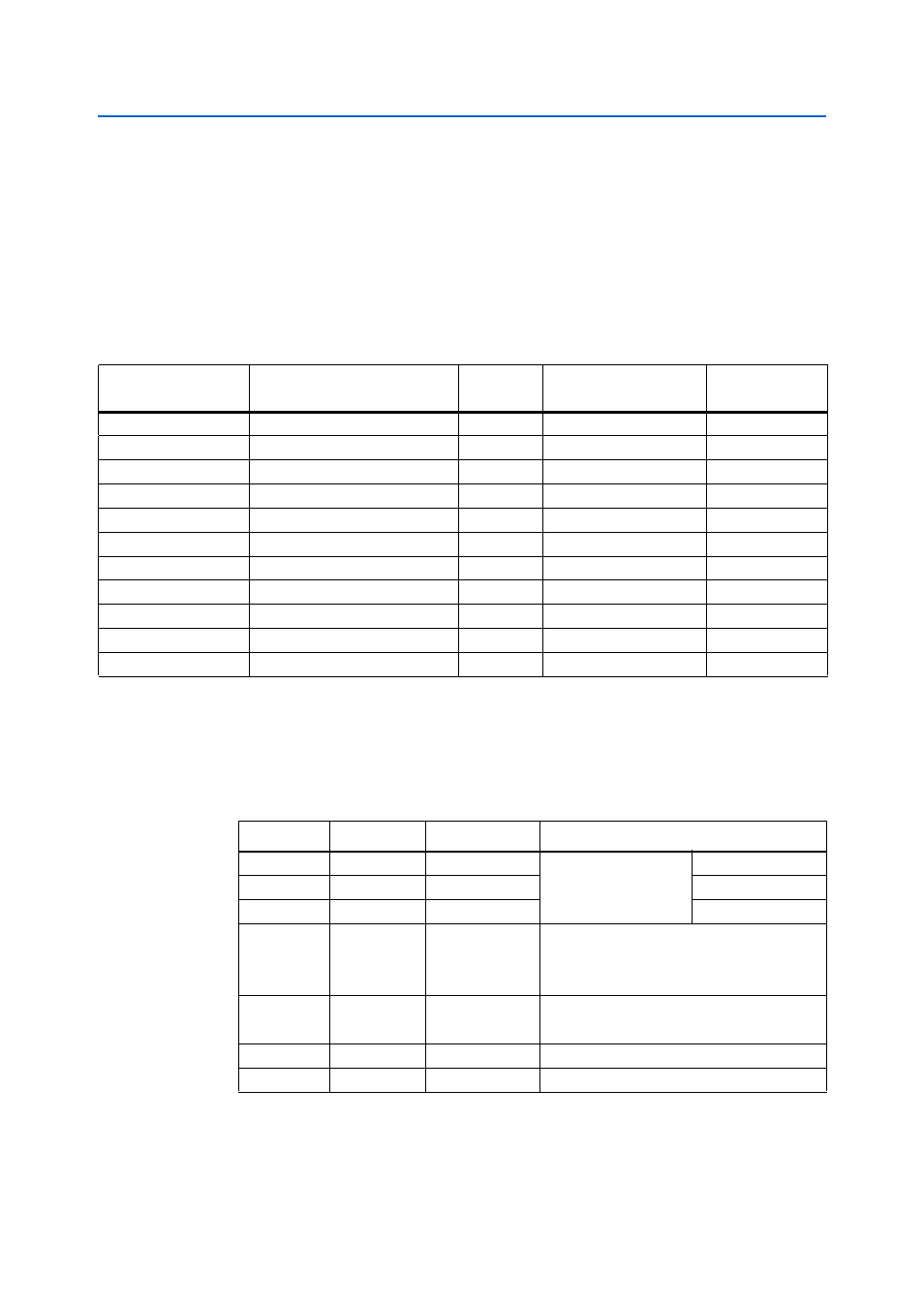
Table 2–36. Character LCD Header I/O
Board
Reference
Description
I/O
Standard
Schematic
Signal Name
Cyclone III Pin
Number
J22 pin 7
LCD data bus bit 0
2.5 V
LCD_DATA0
AA4
J22 pin 8
LCD data bus bit 1
2.5 V
LCD_DATA1
AD1
J22 pin 9
LCD data bus bit 2
2.5 V
LCD_DATA2
V8
J22 pin 10
LCD data bus bit 3
2.5 V
LCD_DATA3
AB5
J22 pin 11
LCD data bus bit 4
2.5 V
LCD_DATA4
AE2
J22 pin 12
LCD data bus bit 5
2.5 V
LCD_DATA5
V5
J22 pin 13
LCD data bus bit 6
2.5 V
LCD_DATA6
V6
J22 pin 14
LCD data bus bit 7
2.5 V
LCD_DATA7
AB3
J22 pin 4
LCD data/command select
2.5 V
LCD_D_Cn
D27
J22 pin 5
LCD write enable
2.5 V
LCD_D_WEn
AC4
J22 pin 6
LCD chip select
2.5 V
LCD_D_CSn
AB24
Table 2–37. Character LCD Display Pin Definitions
Pin Number
Symbol
Level
Function
1
V
DD
—
Power supply
5 V
2
V
SS
—
GND (0 V)
3
V
0
—
For LCD drive
4
RS
H/L
Register select signal
H: Data input
L: Instruction input
5
R/W
H/L
H: Data read (module to MPU)
L: Data write (MPU to module)
6
E
H, H to L
Enable
7~14
DB0~DB7
H/L
Data bus, software selectable 4 or 8 bit mode