Table 2–39 – Altera Cyclone III Development Board User Manual
Page 44
2–34
Chapter 2: Board Components
General User Interfaces
Cyclone III 3C120 Development Board Reference Manual
© March 2009 Altera Corporation
f
For more information about the data sheet and related documentation, visit Lumex at
.
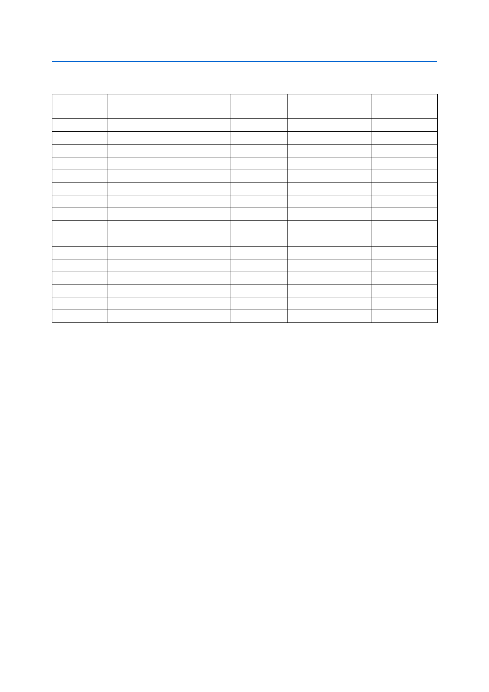
Table 2–39. Graphics LCD Interface I/O
Board
Reference
Description
I/O Standard
Schematic Signal Name
Cyclone III Device
Pin Number
J13 pin 6
LCD data bus bit 0
2.5 V
LCD_DATA0
AA4
J13 pin 7
LCD data bus bit 1
2.5 V
LCD_DATA1
AD1
J13 pin 8
LCD data bus bit 2
2.5 V
LCD_DATA2
V8
J13 pin 9
LCD data bus bit 3
2.5 V
LCD_DATA3
AB5
J13 pin 10
LCD data bus bit 4
2.5 V
LCD_DATA4
AE2
J13 pin 11
LCD data bus bit 5
2.5 V
LCD_DATA5
V5
J13 pin 12
LCD data bus bit 6 _or SCLK
2.5 V
LCD_DATA6
V6
J13 pin 13
LCD data bus bit 7 _or SDATA
2.5 V
LCD_DATA7
AB3
J13 pin 28
Parallel interface selection
_high = 68 series, low = 80 series
2.5 V
LCD_BS1
J13 pin 1
LCD chip select
2.5 V
LCD_CSn
AB24
J13 pin 3
LCD data/command select
2.5 V
LCD_D_Cn
D27
J13 pin 5
LCD read enable
2.5 V
LCD_E_RDn
V7
J13 pin 2
LCD reset
2.5 V
LCD_RSTn
H7
J13 pin 29
LCD parallel/serial data select
2.5 V
LCD_SERn
J13 pin 4
LCD write enable
2.5 V
LCD_WEn
AC4
Note to
:
(1) For the corresponding Cyclone III device pin number, refer to the MAX II device pin-out information in
.