Configuration, Configuration –15, Fpga programming over usb –15 – Altera Cyclone III Development Board User Manual
Page 25: Fpga programming over usb, Advanced jtag settings, refer to table 2–7
Chapter 2: Board Components
2–15
Configuration, Status, and Setup Elements
© March 2009 Altera Corporation
Cyclone III 3C120 Development Board Reference Manual
Configuration
This section discusses FPGA, flash memory, and MAX II device programming
methods supported by the Cyclone III development board.
FPGA Programming Over USB
The FPGA can be configured at any time the board is powered on by using the
USB 2.0 interface and the Quartus II Programmer in JTAG mode.
The JTAG chain is mastered by the embedded USB Blaster function found in the
MAX II device. Only a USB cable is needed to program the Cyclone III FPGA. Any
device can be bypassed by using the appropriate switch on the JTAG control DIP
switch.
1
Board reference SW1 position 5 (SW1.5), labeled MAX0, must be in the closed position
(on) for this feature to properly work. If the SW1 switch is in the closed position, the
parallel flash loader (PFL) megafunction in the MAX II CPLD may try to overwrite
the FPGA image just downloaded over the USB immediately after completion.
For more information about:
■
Advanced JTAG settings, refer to
.
■
The JTAG control switch, refer to
“JTAG Control DIP Switch” on page 2–19
.
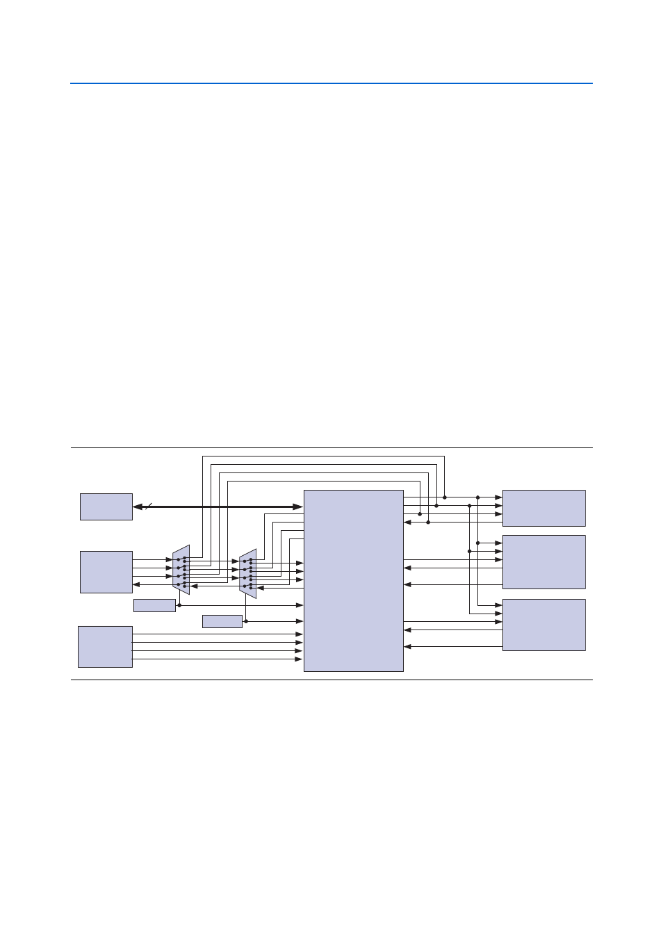
The JTAG header can be used with an external USB-Blaster cable, or equivalent, to
program either the MAX II CPLD or configure the Cyclone III FPGA. Most users of
the Cyclone III development board do not use the JTAG header at all and instead use
a USB cable along with the embedded USB-Blaster. Using an external USB-Blaster
with the JTAG header requires disabling the embedded USB-Blaster function. See
Figure 2–4. JTAG Chain with the MAX II Device and the Cyclone III Device
2.5V
2.5V
2.5V
HSMC Port A
TDI
TDO
TMS
TCK
FPGA
TDI
TDO
TMS
TCK
MAX II
CPLD
PSNTn
HSMC Port B
TDI
TDO
TMS
TCK
PSNTn
TDI
TDO
TMS
TCK
GP
IO P
ins
GP
IO P
ins
GP
IO P
ins
JTAG Control
DIP Switch
FPGA_BYPASS
HSMA_BYPASS
USB 2.0
JTAG
Header
TDO
TDI
TMS
TCK
GP
IO P
ins
Jumper
DEV_SEL
Jumper
JTAG_SEL
HSMA_BYPASS
MAX_EN