High-speed mezzanine connector, High-speed mezzanine connector –42 – Altera Cyclone III Development Board User Manual
Page 52
2–42
Chapter 2: Board Components
Communication Ports and Interfaces
Cyclone III 3C120 Development Board Reference Manual
© March 2009 Altera Corporation
High-Speed Mezzanine Connector
The board contains two HSMC interfaces called Port A and Port B. These HSMC
interfaces support both single-ended and differential signaling. The connector part
number is Samtec ASP-122953-01. The HSM connector interface also allows for JTAG,
SMBus, clock outputs and inputs, as well as power for compatible HSMC daughter
cards.
The HSMC is an Altera-developed specification, which allows users to expand the
functionality of the development board through the addition of HSMC daughter
cards.
f
For more information about the HSMC specification such as signaling standards,
signal integrity, compatible connectors, and mechanical information, visit
.
The HSM connector has 172 total pins, including 120 signal pins, 39 power pins, and
13 ground pins. The ground pins are located between the two rows of signal and
power pins, acting as both a shield and a reference. The HSM connector is based on
the 0.5 mm-pitch QSH/QTH family of high-speed, board-to-board connectors from
Samtec. There are three banks in this connector. Bank 1 has every third pin removed as
is done in the QSH-DP/QTH-DP series. Bank 2 and Bank 3 have all of the pins
populated as done in the QSH/QTH series.
The Cyclone III development board does not use Bank 1 transceiver signals intended
for clock-data-recover (CDR) applications such as PCI Express and Rapid I/O
©
. These
32 pins are left floating. Banks 2 and 3 are fully supported and can be used in two
different configurations. See
The HSMC interface has programmable bi-directional I/O pins that can be used as
2.5-V LVCMOS, which is 3.3-V LVTTL-compatible. These pins can also be used as
various differential I/O standards including, but not limited to LVDS, mini-LVDS,
and RSDS with up to 17-channels full-duplex. Resistor locations are provided for
board-level differential termination on designated receiver pairs, but are not installed
as CMOS utilization of these pins is the default usage model.
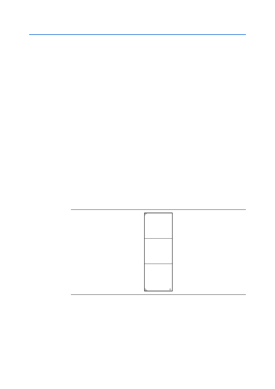
Figure 2–13. HSMC Signal and Bank Diagram
Bank 3
Power
D(79.40)
-or-
LVDS
CLKIN2, CLKOUT2
Bank 2
Power
D(39:0)
-or-
D[3:0] + LVDS
CLKIN1, CLKOUT1
Bank 1
8 TX Channels CD
8 RX Channels CD
JTAG
SMBus
CLKIN0, CLKOUT