Altera Cyclone III Development Board User Manual
Page 56
2–46
Chapter 2: Board Components
Communication Ports and Interfaces
Cyclone III 3C120 Development Board Reference Manual
© March 2009 Altera Corporation
J9 pin 49
LVDS TX 0n or CMOS I/O data bit 6
LVDS or 2.5 V
HSMB_TX_D_N0
J26
J9 pin 50
LVDS RX 0n or CMOS I/O data bit 7
LVDS or 2.5 V
HSMB_RX_D_N0
F28
J9 pin 53
LVDS TX 1p or CMOS I/O data bit 8
LVDS or 2.5 V
HSMB_TX_D_P1
L23
J9 pin 54
LVDS RX 1p or CMOS I/O data bit 9
LVDS or 2.5 V
HSMB_RX_D_P1
G27
J9 pin 55
LVDS TX 1n or CMOS I/O data bit 10
LVDS or 2.5 V
HSMB_TX_D_N1
L24
J9 pin 56
LVDS RX 1n or CMOS I/O data bit 11
LVDS or 2.5 V
HSMB_RX_D_N1
G28
J9 pin 59
LVDS TX 2p or CMOS I/O data bit 12
LVDS or 2.5 V
HSMB_TX_D_P2
M25
J9 pin 60
LVDS RX 2p or CMOS I/O data bit 13
LVDS or 2.5 V
HSMB_RX_D_P2
K25
J9 pin 61
LVDS TX 2n or CMOS I/O data bit 14
LVDS or 2.5 V
HSMB_TX_D_N2
M26
J9 pin 62
LVDS RX 2n or CMOS I/O data bit 15
LVDS or 2.5 V
HSMB_RX_D_N2
K26
J9 pin 65
LVDS TX 3p or CMOS I/O data bit 16
LVDS or 2.5 V
HSMB_TX_D_P3
N25
J9 pin 66
LVDS RX 3p or CMOS I/O data bit 17
LVDS or 2.5 V
HSMB_RX_D_P3
K27
J9 pin 67
LVDS TX 3n or CMOS I/O data bit 18
LVDS or 2.5 V
HSMB_TX_D_N3
N26
J9 pin 68
LVDS RX 3n or CMOS I/O data bit 19
LVDS or 2.5 V
HSMB_RX_D_N3
K28
J9 pin 71
LVDS TX 4p or CMOS I/O data bit 20
LVDS or 2.5 V
HSMB_TX_D_P4
R27
J9 pin 72
LVDS RX 4p or CMOS I/O data bit 21
LVDS or 2.5 V
HSMB_RX_D_P4
L27
J9 pin 73
LVDS TX 4n or CMOS I/O data bit 22
LVDS or 2.5 V
HSMB_TX_D_N4
R28
J9 pin 74
LVDS RX 4n or CMOS I/O data bit 23
LVDS or 2.5 V
HSMB_RX_D_N4
L28
J9 pin 77
LVDS TX 5p or CMOS I/O data bit 24
LVDS or 2.5 V
HSMB_TX_D_P5
R25
J9 pin 78
LVDS RX 5p or CMOS I/O data bit 25
LVDS or 2.5 V
HSMB_RX_D_P5
M27
J9 pin 79
LVDS TX 5n or CMOS I/O data bit 26
LVDS or 2.5 V
HSMB_TX_D_N5
R26
J9 pin 80
LVDS RX 5n or CMOS I/O data bit 27
LVDS or 2.5 V
HSMB_RX_D_N5
M28
J9 pin 83
LVDS TX 6p or CMOS I/O data bit 28
LVDS or 2.5 V
HSMB_TX_D_P6
U25
J9 pin 84
LVDS RX 6p or CMOS I/O data bit 29
LVDS or 2.5 V
HSMB_RX_D_P6
P25
J9 pin 85
LVDS TX 6n or CMOS I/O data bit 30
LVDS or 2.5 V
HSMB_TX_D_N6
U26
J9 pin 86
LVDS RX 6n or CMOS I/O data bit 31
LVDS or 2.5 V
HSMB_RX_D_N6
P26
J9 pin 89
LVDS TX 7p or CMOS I/O data bit 32
LVDS or 2.5 V
HSMB_TX_D_P7
V27
J9 pin 90
LVDS RX 7p or CMOS I/O data bit 33
LVDS or 2.5 V
HSMB_RX_D_P7
P27
J9 pin 91
LVDS TX 7n or CMOS I/O data bit 34
LVDS or 2.5 V
HSMB_TX_D_N7
V28
J9 pin 92
LVDS RX 7n or CMOS I/O data bit 35
LVDS or 2.5 V
HSMB_RX_D_N7
P28
J9 pin 95
LVDS or CMOS clock out
LVDS or 2.5 V
HSMB_CLK_OUT_P1
AC26
J9 pin 96
LVDS or CMOS clock in
LVDS or 2.5 V
HSMB_CLK_IN_P1
J27
J9 pin 97
LVDS or CMOS clock out
LVDS or 2.5 V
HSMB_CLK_OUT_N1
AD26
J9 pin 98
LVDS or CMOS clock in
LVDS or 2.5 V
HSMB_CLK_IN_N1
J28
J9 pin 101
LVDS TX 8p or CMOS I/O data bit 40
LVDS or 2.5 V
HSMB_TX_D_P8
V25
J9 pin 102
LVDS RX 8p or CMOS I/O data bit 41
LVDS or 2.5 V
HSMB_RX_D_P8
P21
J9 pin 103
LVDS TX 8n or CMOS I/O data bit 42
LVDS or 2.5 V
HSMB_TX_D_N8
V26
J9 pin 104
LVDS RX 8n or CMOS I/O data bit 43
LVDS or 2.5 V
HSMB_RX_D_N8
R21
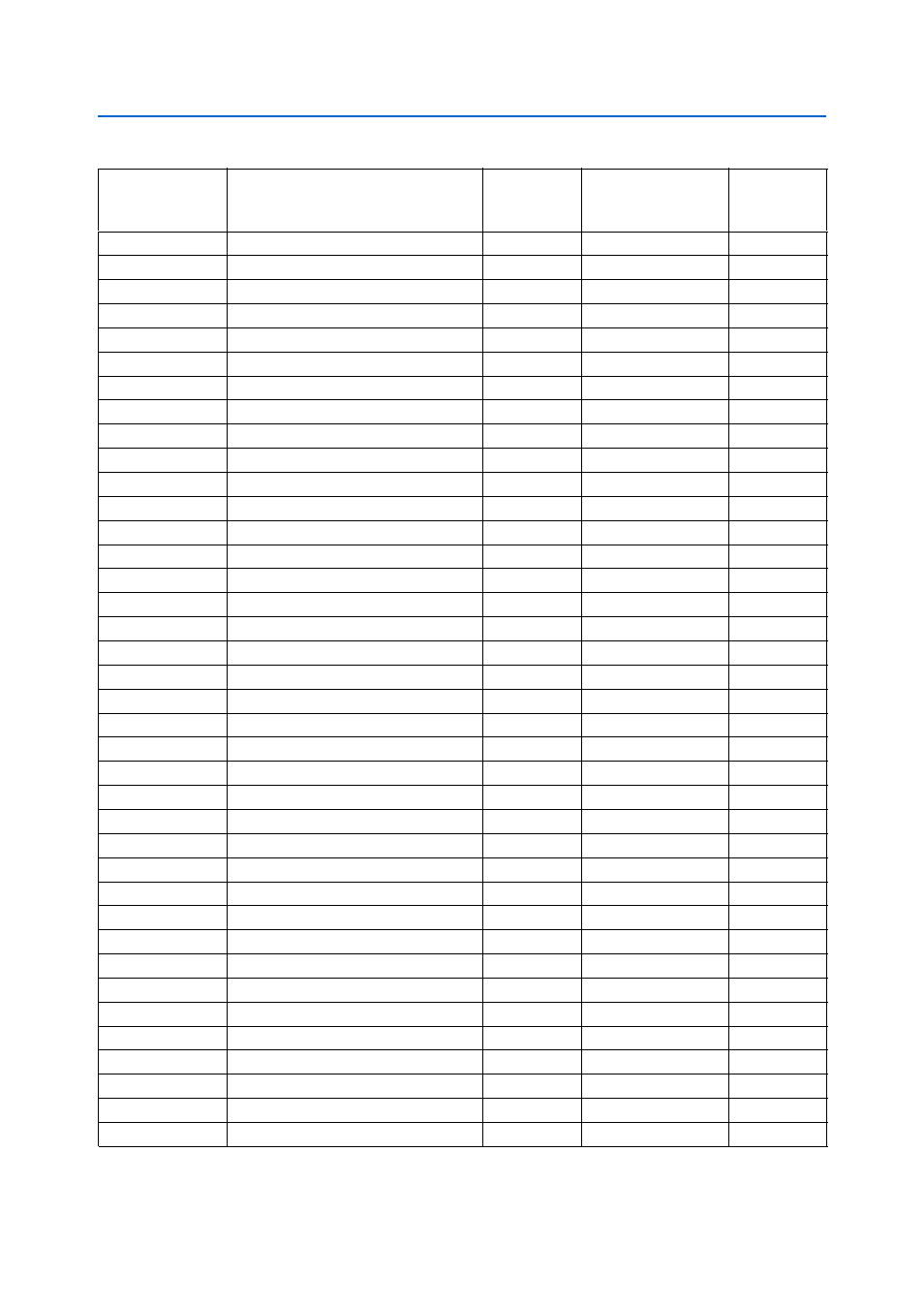
Table 2–48. HSMC Port B Interface Signal Name, Description, and Type (Part 2 of 4)
Board
Reference
Description
I/O Standard
Schematic
Signal Name
Cyclone III
Device Pin
Number