Altera Cyclone III Development Board User Manual
Page 70
2–60
Chapter 2: Board Components
On-Board Memory
Cyclone III 3C120 Development Board Reference Manual
© March 2009 Altera Corporation
defines the flash memory map and lists the signals required for flash
memory. Signal directions are relative to the Cyclone FPGA.
shows the flash device memory map on the Cyclone III development
board. The memory provides non-volatile storage for a minimum of eight FPGA bit
streams, as well as various settings data used for on-board devices such as Ethernet
TCP/IP defaults, PFL configuration bits, and data on the board itself. The remaining
area is designated as user flash area for storage of software binaries and other data
relevant to a user FPGA design.
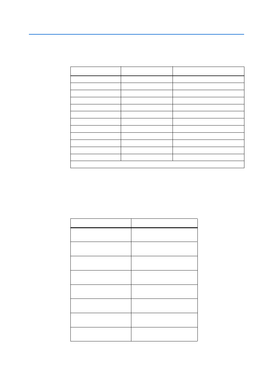
Table 2–57. Flash Memory Map Defined
Signal Name
Description
I/O Standard
FSM_A(24:0)
Address bus (word aligned)
1.8-V LVCMOS out (25 bits)
FSM_D(15:0)
Data bus
N/A (Accounted for in SRAM section)
FLASH_CSn
Chip select
1.8-V LVCMOS out
FLASH_OEn
Output enable
1.8-V LVCMOS out
FLASH_WEn
Write enable
1.8-V LVCMOS out
FLASH_RSTn
Reset
1.8-V LVCMOS out
FLASH_WPn
Write protect
N/A (Tie to VCC)
FLASH_RDYBSYn
Ready/not busy
N/A (Tie to CPLD)
FLASH_BYTEn
Byte/word select
N/A (Tie to CPLD)
VIO
I/O power
1.8 V
VCC
Core power
3.3 V
VSS
Ground
Ground
Cyclone III device I/O totals: 29 1.8 V CMOS I/O pins
Table 2–58. Flash Memory Map (Part 1 of 2)
Name
Address
PFL option bits
0x03FE.0080
0x03FE.0000
Ethernet option bits
0x03FD.FFEF
0x03FC.0000
User space (32 MB)
0x03F9.FFFF
0x0200.0000
Reserved
0x01FF.FFFF
0x01C0.0000
FPGA design 7
0x01BE.EBE1
0x0188.0000
FPGA design 6
0x0186.EBE1
0x0150.0000
FPGA design 5
0x014E.EBE1
0x0118.0000
FPGA design 4
0x0116.EBE1
0x00E0.0000