Altera Stratix II GX PCI Express Development Board User Manual
Page 12
2–2
Reference Manual
Altera Corporation
Stratix II GX PCI Express Development Board
August 2006
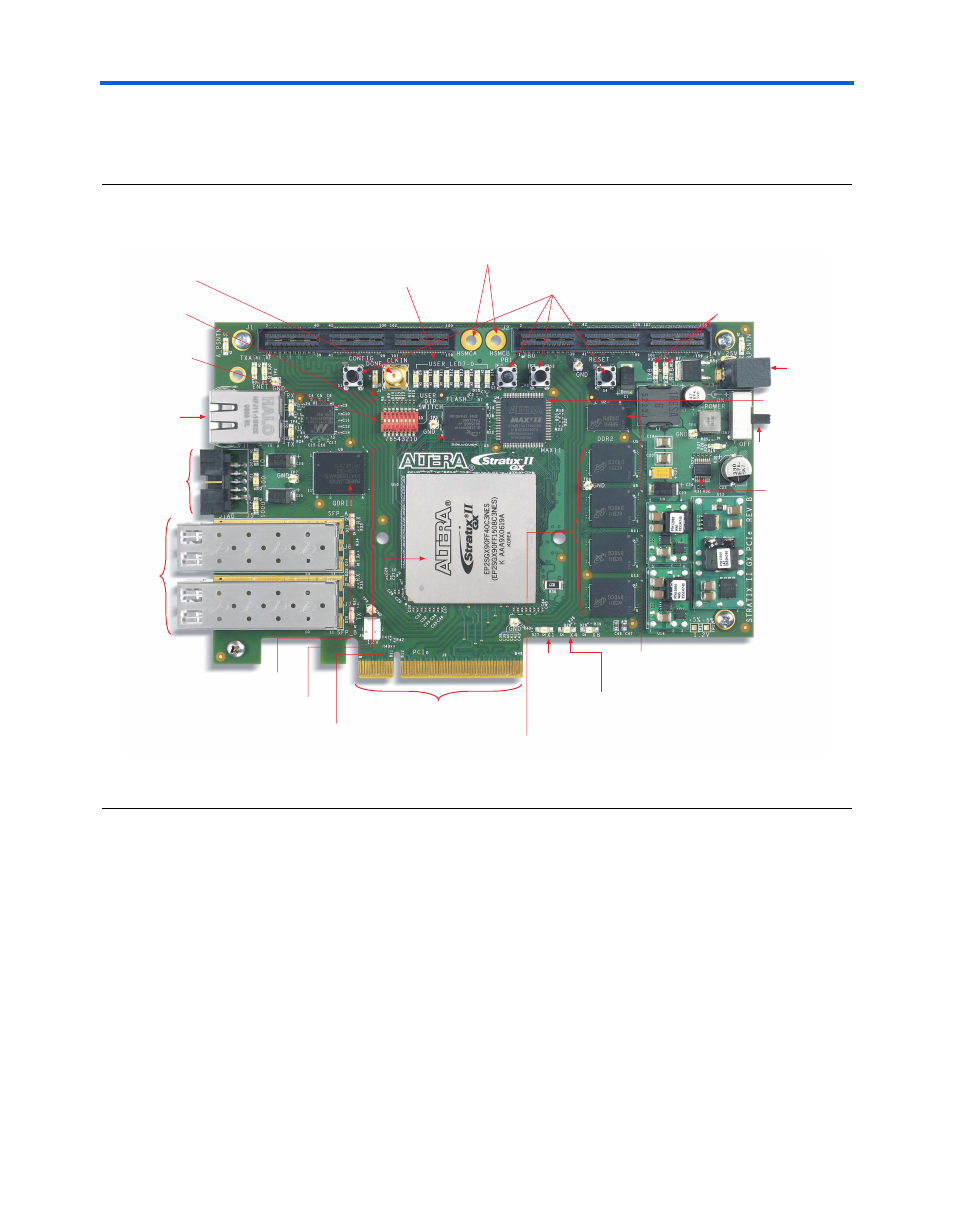
Board Overview
Figure 2–1
shows the top view of the Stratix II GX PCIe development
board.
Figure 2–1. Top View of the Stratix II GX PCIe Development Board
Stratix II GX Device (U10)
Power Switch
(SW1)
Power Supply
Input (J3)
User DIP Switch
Bank (S5)
Flash Device (U3)
User LEDs
(D9 through D16)
MAX II Device
(U4)
High-Speed Mezzanine
Card Interfaces A & B
(J1 and J2)
User Push-Button
Switches (S1 - S4)
DDR2 32 x 16 Mbytes
SDRAM (U5, U8, U11, U13)
Transmit/Receive
Yellow LEDs
(D5 and D6)
DDR2 64 x 8 Mbytes
SDRAM (U2)
Temperature
Sensor With
Alarm (U7)
100-MHz
Crystal (X1)
155.25-MHz
Crystal (X4)
PCI Express x8
Edge Connector
QDRII SRAM (U6)
SFP Ports
A and B
(J6, J7)
JTAG
Header
(J5)
Ethernet RJ-45
Single Port
(RJ1)
HSMC Interface A (J1)
HSMC Interface B (J2)
Configuration Done
LED (D8)
External Clock Input
SMA Connector (J4)