Altera Stratix II GX PCI Express Development Board User Manual
Page 29
Altera Corporation
Reference Manual
2–19
August 2006
Stratix II GX PCI Express Development Board
Board Components & Interfaces
1
For more information about the advanced parallel flash loader
settings, refer to Chapter 2 of the Configuration Handbook,
Configuring Stratix II and Stratix II GX Devices.
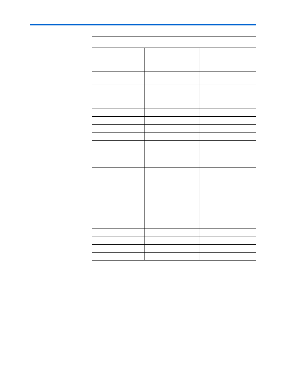
CONFIGn
FPGA nCONFIG pin
connection
1.8-V CMOS in
STATUSn
FPGA nSTATUS pin
connection
1.8-V CMOS in
FLASH_A(24:0)
Flash address bus
1.8-V CMOS out (25 bit)
FLASH_D
Flash data bus
1.8 -V CMOS in/out (16 bit)
FLASH_CEn
Flash chip enable
1.8-V CMOS out
FLASH_OEn
Flash output enable
1.8-V CMOS out
FLASH_WEn
Flash write enable
1.8-V CMOS out
CONFIG_MODE(1:0)
Configuration mode input 1.8-V CMOS in (2 bits)
MSEL(3:0)
FPGA mode select output 1.8-V CMOS out (4 bits)
MAX_EN
Enables operation for
PFL
1.8-V CMOS in
FPGA_PGM(2:0)
Remote configuration
page select
1.8-V CMOS in (3 bits)
DIPSW_PGM(2:0)
DIP switch configuration
page select
1.8-V CMOS in (3 bits)
MAXII_CLK_IN
100-MHz clock input
1.8-V CMOS in
TMS
JTAG mode select
N/A
TDI
JTAG data in
N/A
TDO
JTAG data out
N/A
TCK
JTAG clock
N/A
VCCIO1
I/O bank 1 power
1.8 V
VCCIO2
I/O bank 2 power
1.8 V
VCCINT
Core power
1.8 V
GNDIO
I/O GND
GND
GNDINT
Core GND
GND
Table 2–10. MAX II CPLD Signals & I/O Requirements (Part 2 of 2)
Signal Name
Description
Signal Type