Altera Stratix II GX PCI Express Development Board User Manual
Page 67
Advertising
Altera Corporation
Reference Manual
2–57
August 2006
Stratix II GX PCI Express Development Board
Board Components & Interfaces
1.8 V
FPGA DDR2 I/O
FPGA QDRII I/O
SDRAM VDD 333 MHz
SDRAM VDDQ 333 MHz x72
SRAM 300 MHz
SRAM 300 MHz x36
512 Mb flash
EPM570 CPLD
Total
2.5 V
FPGA HSMC A (LVDS)
FPGA HSMC B (LVDS)
GigE PHY VDDO/H/X
GigE PHY AVDD
Total
3.3 V
FPGA –VCCPD
Oscillator – Marvel GigE ref
Oscillator – PCIe ref
Oscillator – XAUI ref
Oscillator – SONET ref
Clock driver – LVDS buffer
3.3 V-to-SFP module
3.3 V-to-SFP module
3.3 V-to-HMC A
3.3 V-to-HMC B
Linear regulator inputs
Total
5.0 V
FPGA – VCCA (XCVR Analog)
Linear regulator inputs
Total
12 V
12 V-to-card
12 V-to-card
Cooling fan
Switching regulator inputs
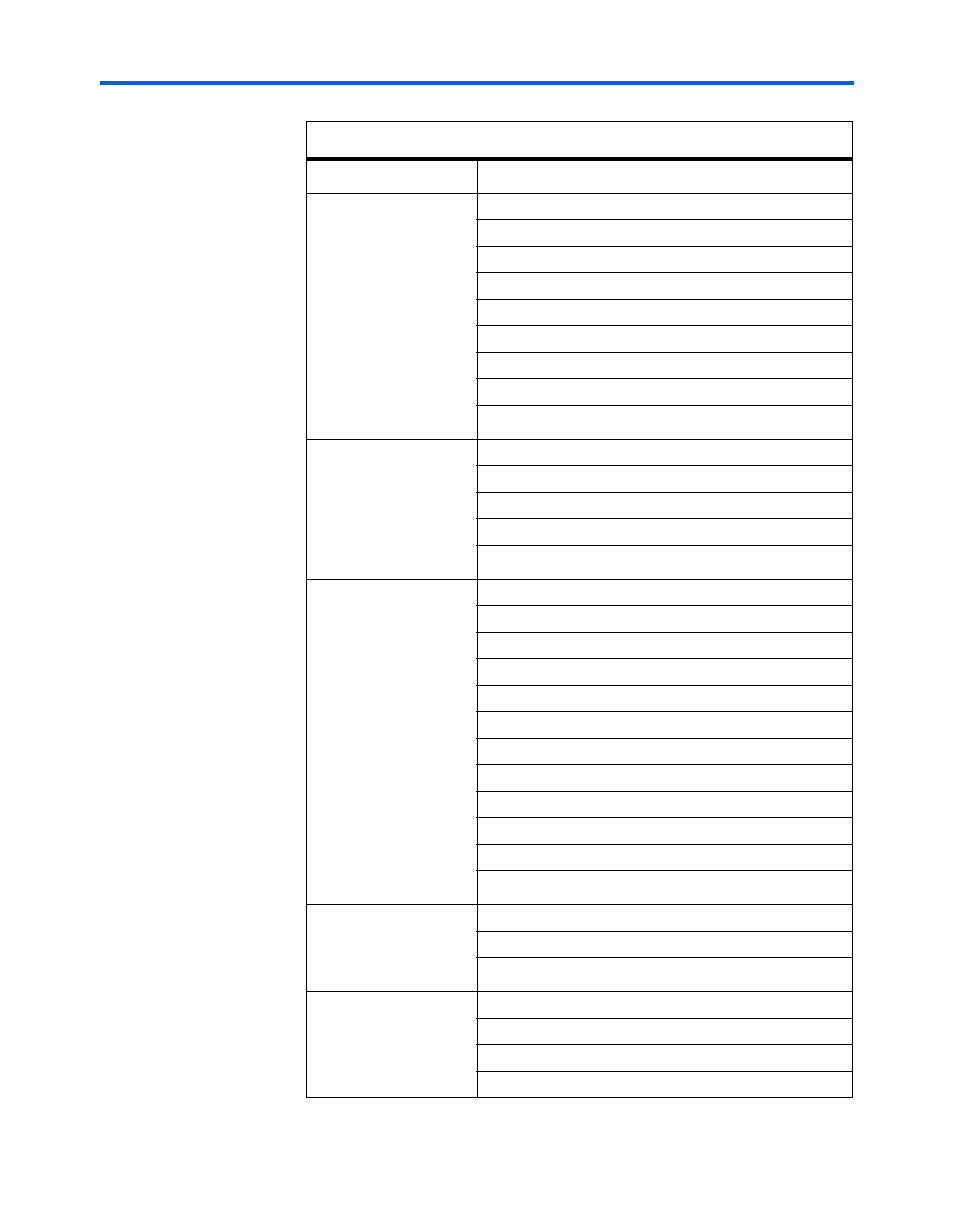
Table 2–36. Power by Rail (Part 2 of 2)
Power Rail
Interface Name
Advertising