Altera Stratix II GX PCI Express Development Board User Manual
Page 37
Altera Corporation
Reference Manual
2–27
August 2006
Stratix II GX PCI Express Development Board
Board Components & Interfaces
The PCIe specification allows for a maximum of 25 W of add-in card
power dissipation. If a card must be over 25 W, then it must power-up in
a state of 25 W or less and wait for the server to register the card as a
high-power device. The card can then ramp up to a maximum of no more
than 40-W total power dissipation.
The x8 edge connector provides 12-V @ 2.1A (max) and 3.3-V @ 3A (max).
There is also a 3.3-V AUX provided for up to 375 mA for wake-on-LAN
and other power sequencing circuitry.
1
These numbers are valid for typical servers or workstations.
They are not valid for stand-alone operation outside of a host
board where all power is derived from an external DC input
jack.
The REFCLKp and REFCLKn signals are the 100-MHz (±300 PPM)
differential reference clock that is driven from a base-board onto the PCIe
add-in card. This is used as the reference clock for the FPGA transceivers
connected to the HSIO data channels. The nominal swing for each
single-ended signal of the differential pair is from 0 V to 700 mV.
The I/O standard is called high-speed current steering logic (HCSL),
which
Figure 2–10
shows along with the Voh/Vol levels that should be
expected as inputs to the card. The clocks are terminated on the host and
should DC couple to the Stratix II GX FPGA.
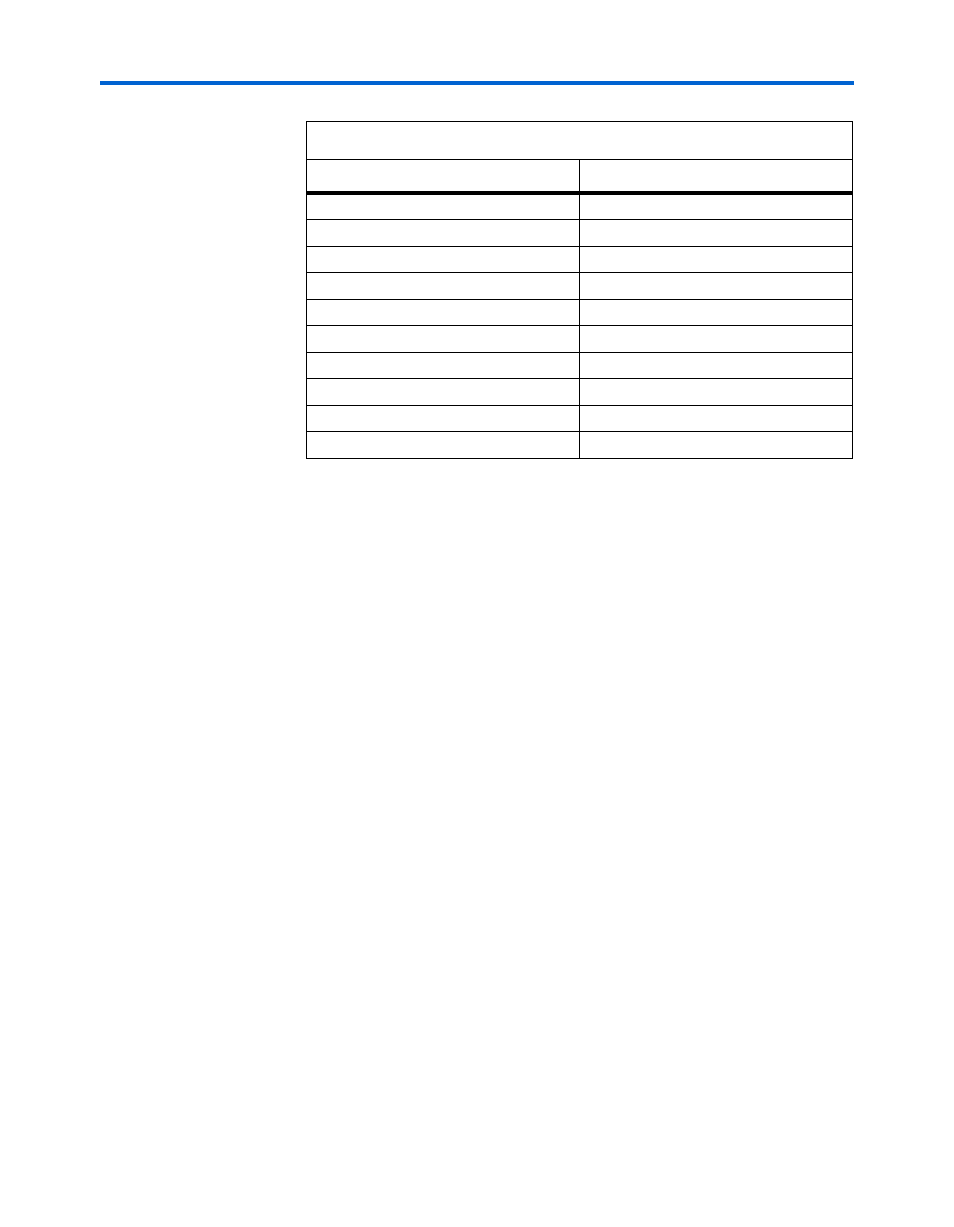
pcie_tx_n[7]
AC5
pcie_tx_p[0]
AG4
pcie_tx_p[1]
AE4
pcie_tx_p[2]
AJ4
pcie_tx_p[3]
AL4
pcie_tx_p[4]
W4
pcie_tx_p[5]
U4
pcie_tx_p[6]
AA4
pcie_tx_p[7]
AC4
pcie_waken
AT10
Table 2–19. PCIe Edge Connector Pin-Out
Schematic Signal Name
Stratix II GX Pin Number