Altera Stratix II GX PCI Express Development Board User Manual
Page 23
Altera Corporation
Reference Manual
2–13
August 2006
Stratix II GX PCI Express Development Board
Board Components & Interfaces
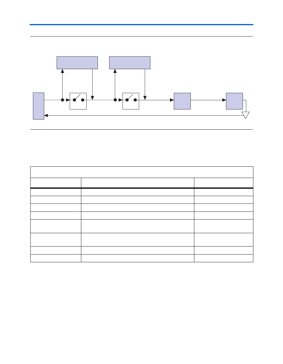
Figure 2–7. JTAG Chain Connections
Because the Stratix II GX device’s TDO pin is located in a 1.8-V I/O bank,
the JTAG chain has a mixture of voltages.
Table 2–5
shows the JTAG chain
signals based on the output.
f
For more information about:
■
JTAG configuration, refer to Appendix A of the PCI Express
Development Kit, Stratix II GX Edition Getting Started User Guide.
■
Programming Altera devices, refer to the Configuration Handbook.
HSMC A
JT
A
G
Header
JTAG_TDI
HSMA_JTAG_TDO
HSMA_JTAG_TDO
DIP Switch
HSMC B
1.8 V
3.3 V
1.8 V
MAX II
CPLD
MAXII_JTAG_TDO
FPGA
3.3 V
3.3 V
DIP Switch
S2GX_JTAG_TDO
Table 2–5. JTAG Chain I/O Signals
Signal Name
Description
Signal Type
JTAG_TCK
JTAG clock (USB-Blaster output)
1.8 V CMOS
JTAG_TMS
JTAG mode select (USB-Blaster output)
1.8 V CMOS
JTAG_TRST
JTAG reset (USB-Blaster output)
1.8 V CMOS
JTAG_TDI
Data output (USB-Blaster output)
1.8 V CMOS
HSMA_JTAG_TDO
HSMC A data output (Bypassable at DIP switch)
LVTTL
(Needs 3.3 V translation)
HSMB_JTAG_TDO
HSMC B data output (Bypassable at DIP switch)
LVTTL
(Needs 3.3 V translation)
MAXII_JTAG_TDO
MAX II data output (Stratix II GX device input)
1.8 V CMOS
S2GX_JTAG_TDO
Stratix II GX device data output (USB-Blaster input)
1.8 V CMOS