Jtag interface, Jtag interface -44, Figure 2–14. example mezzanine cards – Altera Stratix II GX PCI Express Development Board User Manual
Page 53
Altera Corporation
Reference Manual
2–43
August 2006
Stratix II GX PCI Express Development Board
Board Components & Interfaces
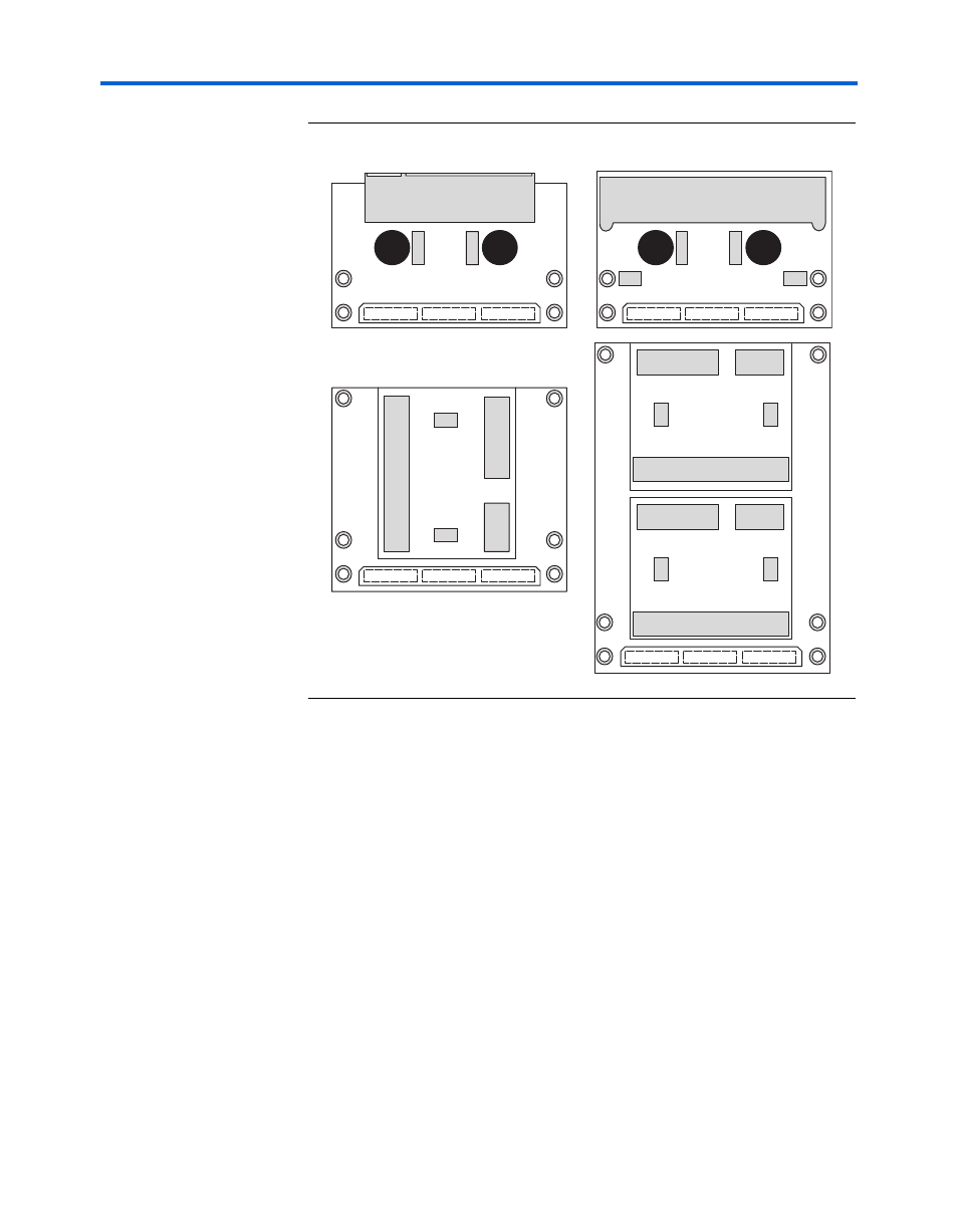
Figure 2–14. Example Mezzanine Cards
JTAG Interface
The board provides a right-angle, 10-pin JTAG header. The JTAG header
protrudes through the front panel of the PCIe card, which positions it well
for internal accessibility while the box is closed. Pin 1 is located on the
side nearest the SFP connectors.
The JTAG header can be used for JTAG-based FPGA programming as
well as communication to a standard computer using a USB-Blaster
download cable. Speeds of approximately 1 Mb/s are achievable using an
SOPC Builder-based Nios II system in the FPGA (via the Quartus II
software SLDHUB primitive) and the default USB-Blaster driver that
Quartus II software installs for JTAG programming and SignalTap
debugging.
f
For more information on the JTAG chain, refer to
x8 PCIe Female
(Right Angle)
AMC Header (type B)
(Right Angle)
Front of Card
fuse
fuse
F2
2 x 20
F3
2 x 10
F1
2 x 7
fuse
fuse
cap
cap
cap
cap
F3
2 x 10
F1
2 x 7
cap
cap
F2
2 x 20
F
ront of Card
F3
2 x 10
F1
2 x 7
cap
cap
F2
2 x 20
F
ront of Card