Max ii cpld configuration controller, Max ii cpld configuration controller -18 – Altera Stratix II GX PCI Express Development Board User Manual
Page 27
Altera Corporation
Reference Manual
2–17
August 2006
Stratix II GX PCI Express Development Board
Board Components & Interfaces
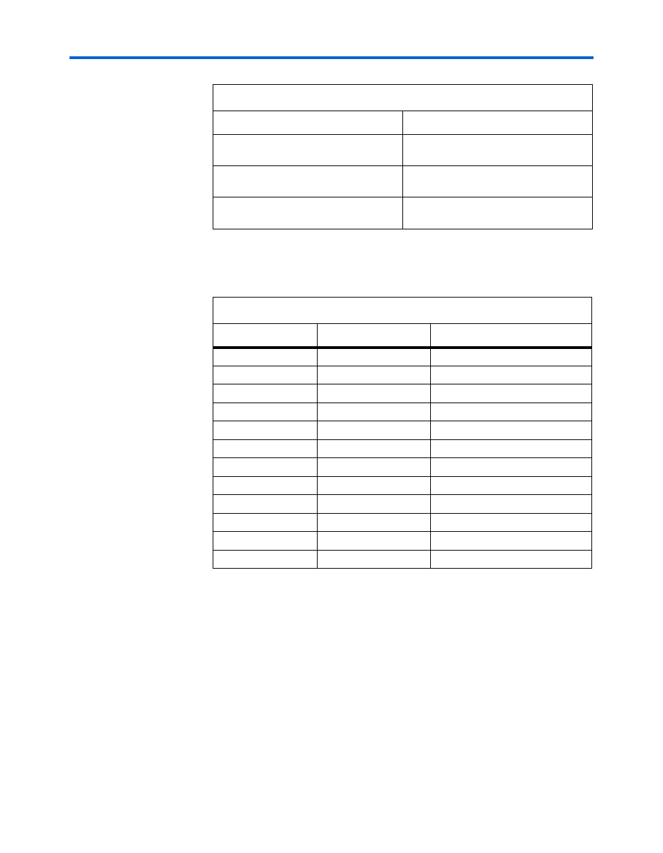
Table 2–9
lists the required signals for the flash memory. Signal directions
are relative to the FPGA as far as direction and signaling standard.
MAX II CPLD Configuration Controller
The MAX II CPLD is exclusively used for FPGA configuration and flash
programming. The target MAX II device is a 1.8 V-only EPM570GT100.
The PFL megafunction is the basis for the MAX II CPLD design.
When using the default PFL megafunction, keep in mind that it may need
to be modified to meet PCIe specification requirements. Specifically, the
PCIe specification states that a device be ready to enter the link training
state within 80 ms of the end of a fundamental reset (release of the
PERSTn
pin). This can be a power-on-reset where the PWR GOOD signal is
FPGA Design 2
0x00BF.FFFF
0x0080.0000
FPGA Design 1
0x007F.FFFF
0x0040.0000
FPGA Design 0 (default)
0x003F.FFFF
0x0000.0000
Table 2–9. Flash Interface I/O
Signal Name
Description
Signal Type
FLASH_A(24:0)
Address bus
1.8-V CMOS out (25 bit)
FLASH_D(15:0)
Data bus
1.8-V CMOS out (16 bit)
FLASH_CEn
Chip enable
1.8-V CMOS out
FLASH_RESETn
Reset
1.8-V CMOS out
FLASH_OEn
Output enable
1.8-V CMOS out
FLASH_WEn
Write enable
1.8-V CMOS out
FLASH_WPn
Write protect
N/A (Tie to VCC)
FLASH_RDYBSYn
Ready/not busy
1.8-V CMOS in (Tie to VCC)
FLASH_BYTEn
Byte/word select
1.8-V CMOS out (Tie to VCC)
VIO
I/O power
1.8-V
VCC
Core power
3.3-V
VSS
Ground
Ground
Table 2–8. Example Flash Memory Map (Part 2 of 2)
Memory Block
Address