Altera Stratix II GX PCI Express Development Board User Manual
Page 28
2–18
Reference Manual
Altera Corporation
Stratix II GX PCI Express Development Board
August 2006
Configuration Schemes and Status LEDs
asserted within 100 ms of power levels being at the minimum level and
then an additional 100 ms for the reference clocks to stabilize. The
following text is an excerpt from the PCIe specification:
PCI Express Power-On-Reset Timing Specifications
The first set of rules addresses requirements for component devices:
■
A component must enter the initial active Link Training state within 80 ms
of the end of Fundamental Reset (Link Training is described in Section
4.2.4).
●
Note: In some systems, it is possible that the two components on a Link
may exit Fundamental Reset at different times. Each component must
observe the requirement to enter the initial active Link Training state
within 80 ms of the end of Fundamental Reset from its own point of
view.
■
On the completion of Link Training (entering the DL_Active state, see
Section 3.2), a component must be able to receive and process TLPs and
DLLps.
The second set of rules addresses requirements placed on the system:
■
To allow components to perform internal initialization, system software
must wait for at least 100 ms from the end of a reset of one or more devices
before it is permitted to issue Configuration Requests to those devices.
●
A system must guarantee that all components intended to be software
visible at boot time are ready to receive Configuration Requests within
100 ms of the end of Fundamental Reset at Root Complex - how this is
done is beyond the scope of this specification.
The MAX II CPLD is part of the board’s JTAG chain and can be
programmed using the Quartus II Programmer and a USB-Blaster cable.
The same JTAG interface is also used to program flash images.
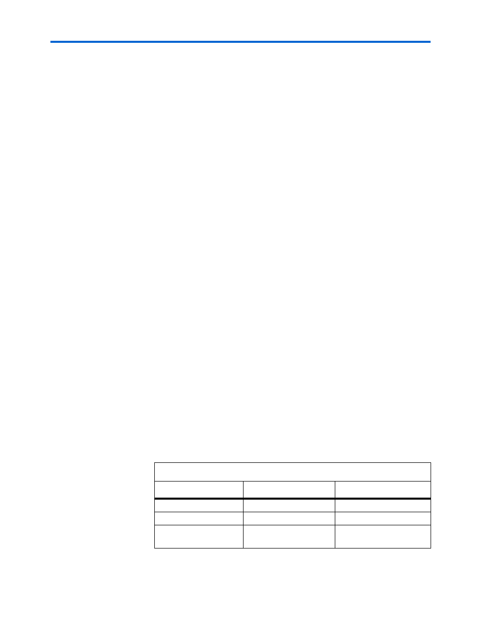
Table 2–10
lists the required MAX II CPLD signals and the corresponding
PFL megafunction design I/O requirements. Signal directions are relative
to the CPLD as far as direction and signaling standard.
Table 2–10. MAX II CPLD Signals & I/O Requirements (Part 1 of 2)
Signal Name
Description
Signal Type
FPGA_CONFIG_DCLK
Configuration clock
1.8-V CMOS out
FPGA_CONFIG_D(7:0)
Configuration data bus
1.8-V CMOS out (8 bits)
CONF_DONE
FPGA CONF_DONE pin
connection
1.8-V CMOS in