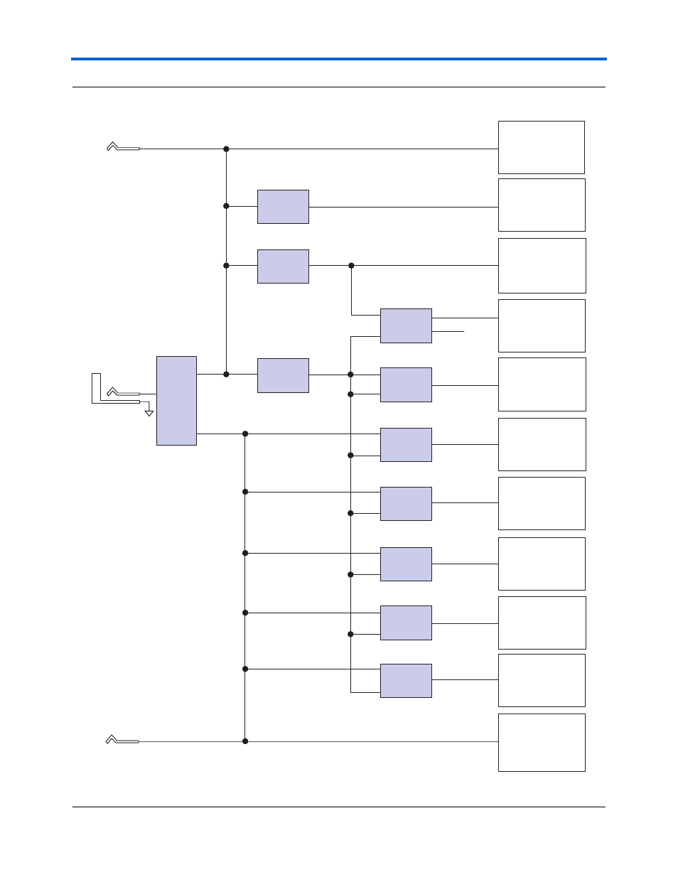
Figure 2–15. power distribution system – Altera Stratix II GX PCI Express Development Board User Manual
Page 69
Altera Corporation
Reference Manual
2–59
August 2006
Stratix II GX PCI Express Development Board
Board Components & Interfaces
Figure 2–15. Power Distribution System
Custom
Dual
Output
Switching
Regulator
12 V
DC Input
14 V - 20 V
12V = PCIe Motherboard
12A Switching
Regulator
Module
12-V PowerNet
HMCA
HMCB
Cooling Fan
1.2-V Partial Plane
Stratix II GX VCCint
Stratix GX XCVR PCS
Marvell PHY
6A Switching
Regulator
Module
Linear
V
IN
V
BIAS
1.8-V Partial Plane
Stratix II GX VCCio
DDR2 SDRAM
QDRII SRAM
MAXII and FLASH
3.3-V Partial Plane
Stratix II GX VCCpd
HMCA, HMCB
SFPA, SFPB
Oscillators, Driver
VTT
PowerNet
Memory Termination
XCVR_VCCA
PowerNet
TXVR VCCA
XCVR_VCCHTX
PowerNet
XCVR VCCG
XCVR_VCCR
PowerNet
XCVR VCCR
XCVR_VCCT
PowerNet
XCVR VCCT
XCVR VCCL
VCCA
PowerNet
Stratix II GX
EPLL/FPLL
2.5-V
Partial Plane
Stratix II LVDS VCCio
Marvell PHY
6A Switching
Regulator
Module
3.3 V = PCIe Motherboard
0.9 V
VREF
3.3 V
2.5 V
1.5 V
12 V
1.8 V
5.0 V
1.2 V
3.3 V
33 mA
92 mA
33 mA
33 mA
1.2 V
33 mA
1.2 V
33 mA
1.2 V
33 mA
Linear
V
IN
V
BIAS
Linear
V
IN
V
BIAS
Linear
V
IN
V
BIAS
Linear
V
IN
V
BIAS
Linear
V
IN
V
BIAS
Linear
V
IN
V
BIAS