Altera Stratix II GX PCI Express Development Board User Manual
Page 14
2–4
Reference Manual
Altera Corporation
Stratix II GX PCI Express Development Board
August 2006
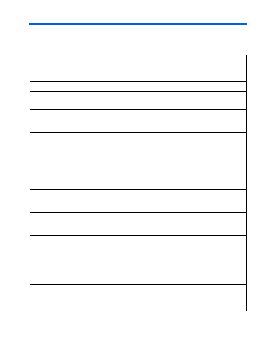
Board Overview
describes the components and lists their corresponding board
references.
Table 2–1. Stratix II GX PCIe Development Board Features
Component/
Interface
Board
Reference
Description
Page
Featured Device
Stratix II GX FPGA
U10
FF1508 FPGA in a 1508-pin FineLine BGA
®
package.
Clocks
100 MHz
X1
100-MHz oscillator
25 MHz
X2
25-MHz crystal
156.25 MHz
X3
156.25-MHz oscillator
155.52 MHz
X4
155.52-MHz oscillator
SMA clock input
J4
SMA connector that allows the provision of an external clock
to the Stratix II GX device’s transceivers.
Configuration and Status
Board configuration
DIP switch
S6
DIP switch that controls the FPGA configuration settings.
Status LEDs
D1, D2, D8,
D19-D22
LEDs that display power and configuration status.
Channel activity LEDs
D3-D6, D17,
D18, D23-D29
LEDs that display RX and TX transceiver channel activity.
User I/O
Push-button switches
S1-S4
User-defined push-button switches.
User LEDs
D9-D16
User-defined LEDs.
8-pin DIP switch
S5
User-defined DIP switches.
JTAG header
J5
10-pin header for JTAG-based FPGA communication.
Interfaces
PCIe edge connector
J9
A x8 (8 channel) PCI Express edge connector for insertion
into PCI Express-based host platforms.
Ethernet RJ-45
RJ1
The RJ-45 jack is for Ethernet cable connection. The
connector is fed by a 10/100/1000 base T PHY device with a
GMII interface to the Stratix II GX device.
SFP A
J6
Small form pluggable cage allows for the connection of SFP
modules.
SFP B
J7
Small form pluggable cage allows for the connection of SFP
modules.