Altera Stratix II GX PCI Express Development Board User Manual
Page 42
2–32
Reference Manual
Altera Corporation
Stratix II GX PCI Express Development Board
August 2006
Standard Communication Ports
Because the GMII interface bank’s voltage level for the FPGA is only
1.8 V, voltage translators are required to “up-convert” the 1.8 V FPGA
outputs using FXL4T245 dual-voltage buffers. The 2.5-V CMOS outputs
from the Marvell 88E1111 are over-driving the FPGA input pins (2.5 V
CMOS driving 1.8 V buffer inputs). The source-synchronous timing is
affected by this up-conversion as the buffers have their own pin-to-pin
delay specification.
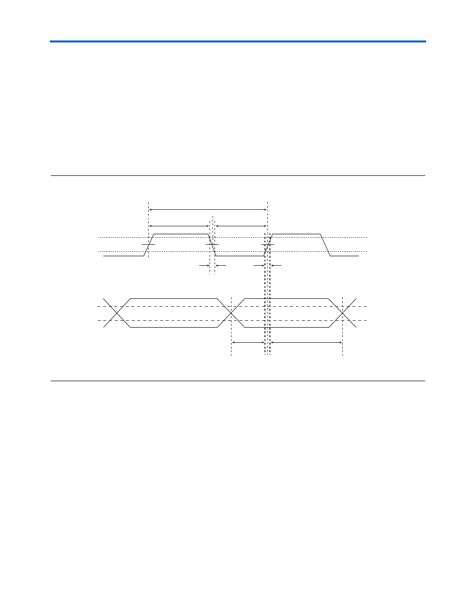
Figure 2–12
shows the source-synchronous GMII interface TX timing
diagram.
Figure 2–12. Marvell 88E1111 GMII TX Timing Diagram
The board provides an internal MAC core as an application layer
interface for user designs. You can test it by accessing the stack provided
as an Altera SOPC Builder component.
An IP core is also available from the Altera Megafunctions Partner
Program (AMPP
SM
) partner MorethanIP. The MorethanIP core has been
used and tested on an existing Altera daughter card using the Nios II
processor core and the MorethanIP TCP/IP driver software for the Nios II
processor.
1
Additional GigE ports can be added using plug-in modules on
the board’s SFP connectors for either copper or optical
applications.
V
IH_GMII
(Min.)
T
P_GMII_GTX_CLK
T
H_GMII_GTX_CLK
T
R_GMII_GTX_CLK
T
F_GMII_GTX_CLK
T
R_GMII_GTX_CLK
T
SU_GMII_GTX_CLK
T
HD_GMII_GTX_CLK
GTX_CLK
TDX[7:0]
TX_EN
TX_ER
V
IL_GMII
(Max.)
V
IH_GMII
(Min.)
V
IL_GMII
(Max.)