Altera Stratix II GX PCI Express Development Board User Manual
Page 25
Altera Corporation
Reference Manual
2–15
August 2006
Stratix II GX PCI Express Development Board
Board Components & Interfaces
f
For information about board-supported FPGA configuration schemes,
refer to
Table 2–7 on page 2–15
.
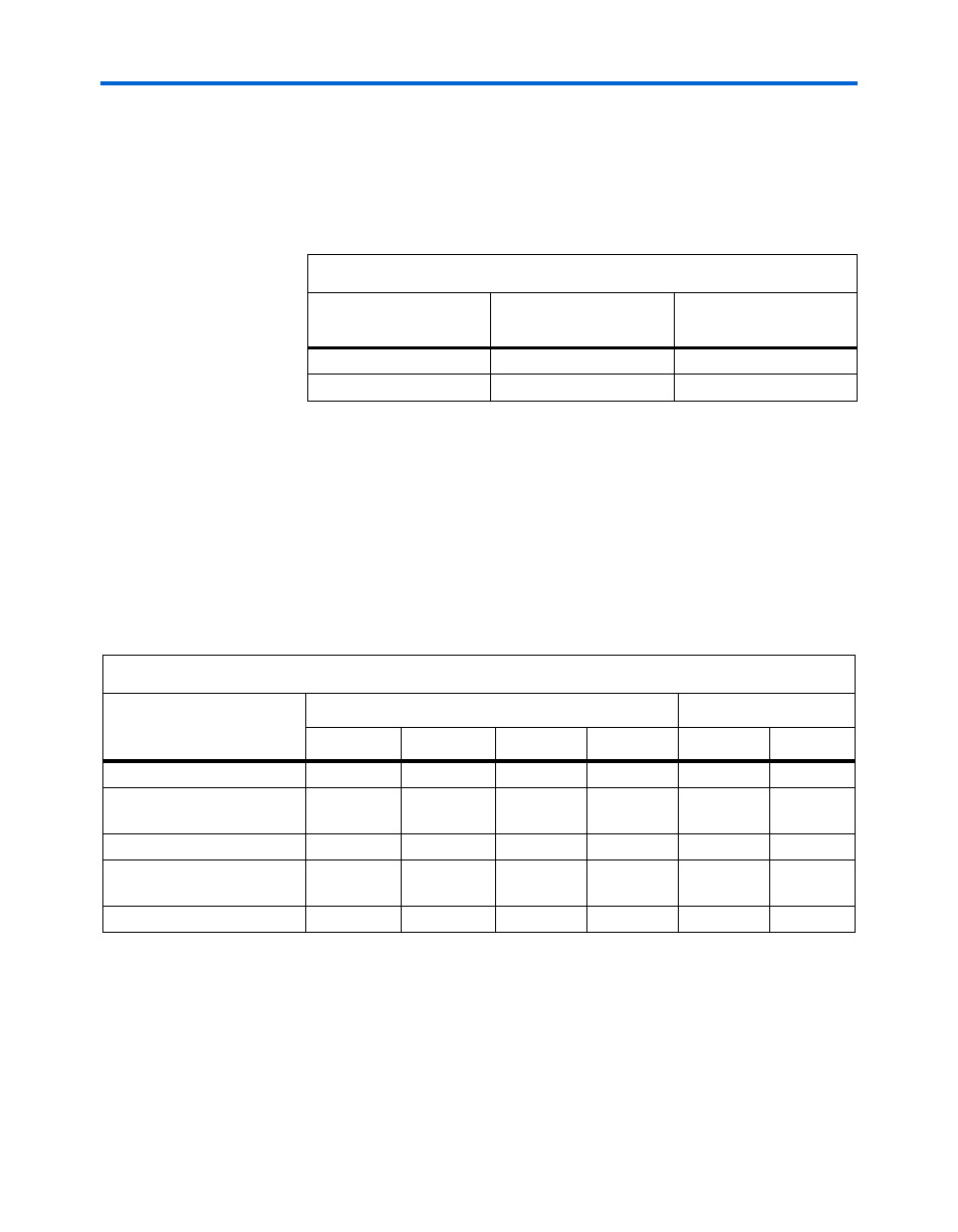
Table 2–6
shows configuration file sizes for board-supported Stratix II GX
devices.
1
The 512-MB, on-board flash device is able to store either eight
designs of the EP2SGX90 device plus 32-Mbytes of additional
files, or eight designs of the EP2SGX130 device and 16-Mbytes of
additional files.
Table 2–7
shows the board-supported FPGA configuration schemes.
1
The same DIP switch used to select the configuration mode will
also have RUnLU pin control as well as some JTAG chain options.
Refer to the
“General User Interfaces” on page 2–21
for more
information on the DIP switch.
Table 2–6. Configuration File Sizes
Device
Configuration File Size
(Mb)
(1)
Compressed File Size
(Mb)
(2)
EP2SGX90
25,699,104
9,251,677
EP2SGX130
37,325,760
13,437,273
Notes to
Table 2–6
:
(1)
This is a preliminary value based on both the EP2SGX90 and EP2SGX130 devices.
(2)
This value assumes average reduction of 64%.
Table 2–7. Board-Supported FPGA Configuration Schemes & MSEL Settings
Configuration Scheme
FPGA MSEL Settings (From MAX II CPLD)
DIP Switch Settings
MSEL-3
MSEL-2
MSEL-1
MSEL-0
Mode-1
Mode-0
Fast passive parallel (FPP)
0
0
0
0
0
0
Remote system upgrade
(RSU) FPP
(1)
0
1
0
0
0
1
FPP with decompression
1
0
1
1
1
0
RSU FPP with
decompression
(1)
1
1
0
0
1
1
JTAG
N/A
N/A
N/A
N/A
N/A
N/A
Note to
Table 2–7
:
(1)
The RSU scheme uses the FPGA PGM(2:0) outputs page-select pins.