Fpp configuration, Fpp configuration -14 – Altera Stratix II GX PCI Express Development Board User Manual
Page 24
2–14
Reference Manual
Altera Corporation
Stratix II GX PCI Express Development Board
August 2006
Configuration Schemes and Status LEDs
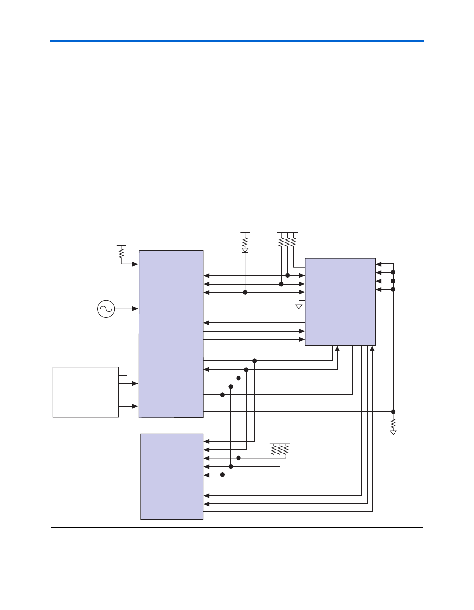
FPP Configuration
Many applications involving PCIe require that a device being configured
enter the user operation mode before the computer containing the PCIe
card recognizes the PCIe bus. To facilitate this fast configuration scheme,
an on-board configuration controller is provided. The configuration
controller consists of a MAX II CPLD and a page-mode flash memory
device. When power is applied to the board, the MAX II CPLD loads a
configuration from the flash device into the Stratix II GX device in the
FPP mode. The MAX II CPLD holds the configuration state machine and
the flash memory holds the non-volatile configuration bit streams.
Figure 2–8
shows the FPP configuration scheme.
Figure 2–8. FPP Configuration Scheme
FPGA_nSTATUS
FPGA_nCONFIG
FPGA_CONF_DONE
FPGA_PGM[2:0]
FPGA_DATA[7:0]
FPGA_DCLK
FLASH_A[24:0]
FLASH_D[15:0]
FLASH_CEn
FLASH_OEn
FLASH_WEn
MSEL[3:0]
MAX_EN
MAX II CPLD
FPGA_RSTn
FPGA_BYTEn
FPGA_RYBYn
FLASH_A[25:0]
FLASH_D[15:0]
FLASH_CEn
FLASH_OEn
FLASH_WEn
CFI FLASH
RUnLU
CONFIG_MODE[1:0]
DIPSW+PGM[2:0]
DIP Switch
100MHz
1.8V
MSEL3
MSEL2
MSEL1
MSEL0
Stratix II GX Device
INIT_DONE
nSTATUS
CONF_DONE
nCE
nCONFIG
RUnLU
10 kohm
10 kohm
10 kohm
LED
from DIPSW
DATA[7:0]
DCLKFLASH Interface
PGM[2:0]
1.8V
1.8 V
1.8V