Flash memory configuration file storage, Flash memory configuration file storage -17 – Altera Stratix II GX PCI Express Development Board User Manual
Page 26
2–16
Reference Manual
Altera Corporation
Stratix II GX PCI Express Development Board
August 2006
Configuration Schemes and Status LEDs
This section discusses:
■
Flash memory configuration file storage
■
MAX II configuration controller
Flash Memory Configuration File Storage
A 512-MB Spansion flash memory device is used to store configuration
files for the FPGA as well as any other necessary data. The target device
is a Spansion S29GL512N in a BGA package, which supports CFI flash
commands.
The flash memory map is determined by the MAX II CPLD design, which
is based on the parallel flash loader (PFL) megafunction. The PFL
megafunction takes up to eight Quartus II programmer object files (.pof)
and stacks them into a single image to be written to flash memory using
the Quartus II Programmer and a USB-Blaster cable. This is done via the
JTAG header and the MAX II CPLD to flash memory.
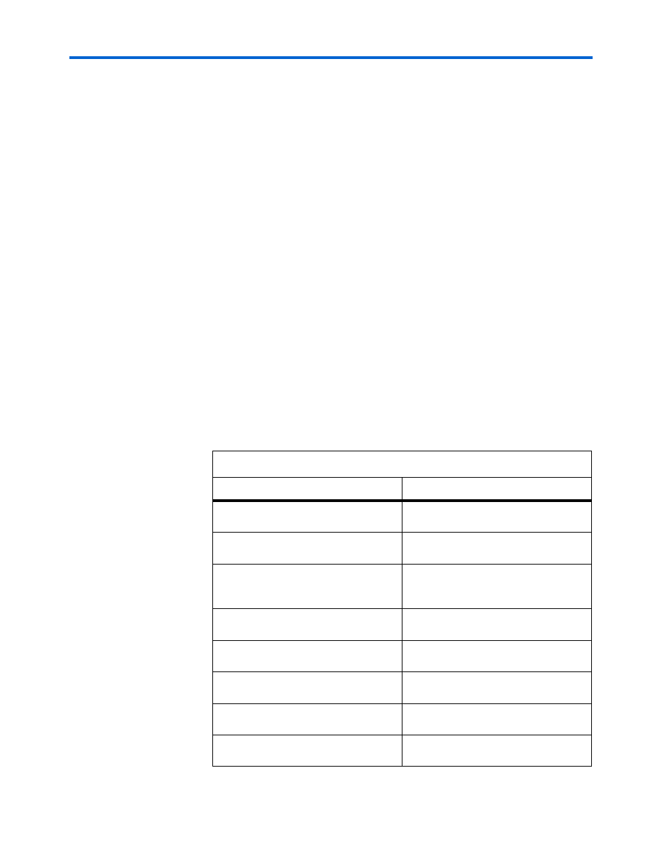
Table 2–8
lists an example flash memory map. The sizes of various blocks
may change based on the settings used, such as the compression setting,
in the Quartus II Programmer. The PFL Option Bits are used by the
MAX II CPLD design to store the address of the POF files. The Ethernet
Option Bits are used by MAC IP for IP and MAC address storage.
Table 2–8. Example Flash Memory Map (Part 1 of 2)
Memory Block
Address
PFL Option Bits
0x03FF.FFFF
0x03FF.FFF0
Ethernet Option Bits
0x03FF.FFEF
0x03FF.FFE0
User Space
(16MB-32MB)
0x03FF.FFDF
0x0200.0000
FPGA Design 7
0x01FF.FFFF
0x01C0.0000
FPGA Design 6
0x01BF.FFFF
0x0180.0000
FPGA Design 5
0x017F.FFFF
0x0140.0000
FPGA Design 4
0x013F.FFFF
0x0100.0000
FPGA Design 3
0x00FF.FFFF
0x00C0.0000