Clocking circuitry, Clocking circuitry -11 – Altera Stratix II GX PCI Express Development Board User Manual
Page 21
Altera Corporation
Reference Manual
2–11
August 2006
Stratix II GX PCI Express Development Board
Board Components & Interfaces
Clocking
Circuitry
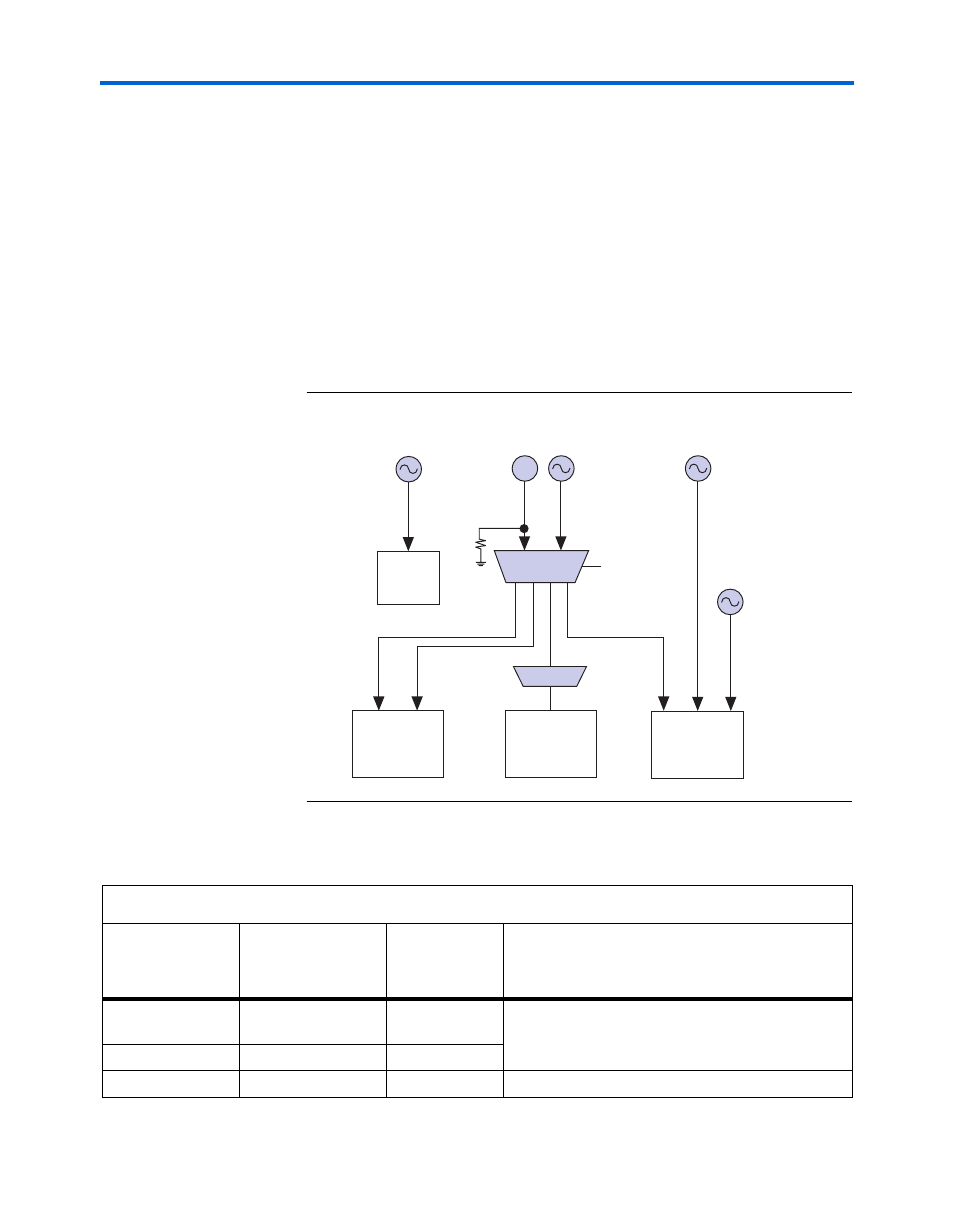
Three oscillators of 100 MHz, 156.25 MHz, and 155.52 MHz are used for
clocking the Stratix II GX transceivers and user logic. A fourth oscillator
of 25.000 MHz +/- 50 ppm is used as a reference clock for the Marvel
10/100/1000 Ethernet PHY device per manufacturing recommendations.
When the board is not plugged into a host board, the 100-MHz oscillator
is used to support the transceiver reference clock for PCIe applications.
Figure 2–6
shows the oscillator driving through a four-output LVDS
buffer to a variety of loads. The buffer can either be driven from the
100-MHz oscillator or from the SMA clock input for custom frequencies.
Pin 10 on the board configuration DIP switch controls what clock feeds
the buffer (see
“Configuration DIP Switch (S6)” on page 2–23
).
Figure 2–6. Oscillator Clocking Diagram
lists the board’s clock distribution system.
152.520 MHz
SMT OSC
156.250 MHz
SMT OSC
100 MHz
SMT OSC
MAX II
Configuration
Controller
88e1111
GigE
PHY
Stratix II GX
Enhanced PLL
Inputs
Stratix II GX
Enhanced PLL
Inputs
Clock Buffer
OSC B
25 MHz
SMT OSC
OSC A
LVTTL
LVTTL
LVDS
LVDS
LVDS
LVDS
LVDS
LVDS
LVTTL
SMA
R
T
All A/C Coupled
Translator
CLK_SEL
Table 2–4. Stratix II GX PCIe Development Board Clock Distribution (Part 1 of 2)
Frequency
Signal Name
Signal
Originates
From
Signal Propagates To
100 MHz
100M_OSC_P
100M_OSC_N
X1
U21 (ICS8543 clock buffer), Pins 4 and 5
User input
SMA clock input
J4
25 MHz
ENET_25M_CLK
X2
Ethernet PHY