Gigabit ethernet (gige) interface (rj1), Gigabit ethernet (gige) interface (rj1) -29, Figure 2–10. pci express reference clock levels – Altera Stratix II GX PCI Express Development Board User Manual
Page 38
Advertising
2–28
Reference Manual
Altera Corporation
Stratix II GX PCI Express Development Board
August 2006
Standard Communication Ports
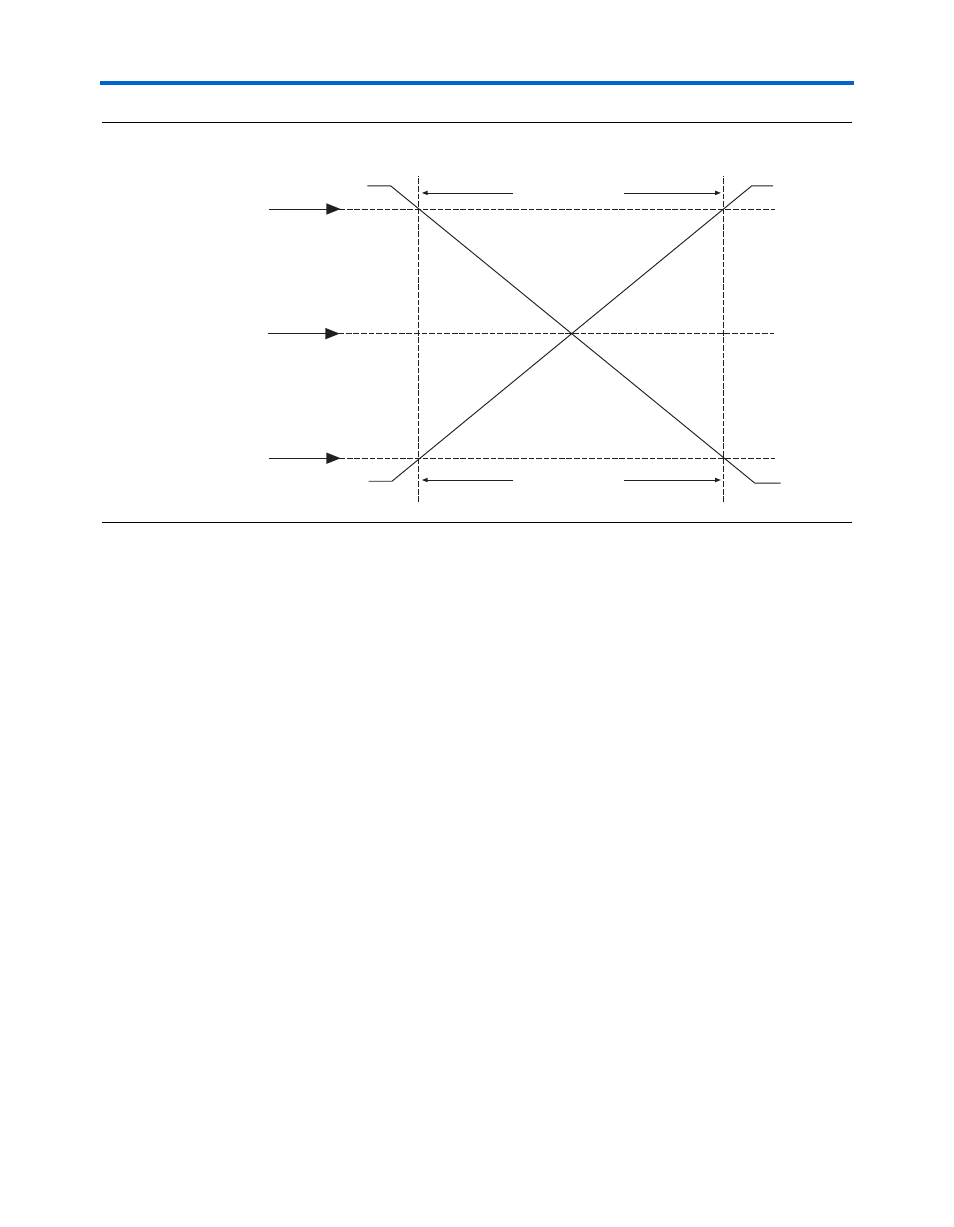
Figure 2–10. PCI Express Reference Clock Levels
Gigabit Ethernet (GigE) Interface (RJ1)
The board’s GigE interface is implemented with an RJ-45 jack and a
dedicated 10/100/1000 base-T, auto-negotiating Ethernet physical
device. The media access controller (MAC) layer must be implemented in
the FPGA and connect to the PHY device through either the Gigabit
medium independent interface (GMII) or medium independent interface
(MII).
Figure 2–11
shows the interface between the Stratix II GX device’s MAC
and the GigE PHY layer.
V
OH
= 0.525V
Cloc
k#
T
RISE
(Clock)
V
CROSS
V
OL
= 0.175V
T
FALL
(Clock#)
Cloc
k
Advertising