Avalon-to-pci write requests – Altera PCI Compiler User Manual
Page 299
Altera Corporation
User Guide Version 11.1
7–31
October 2011
Functional Description
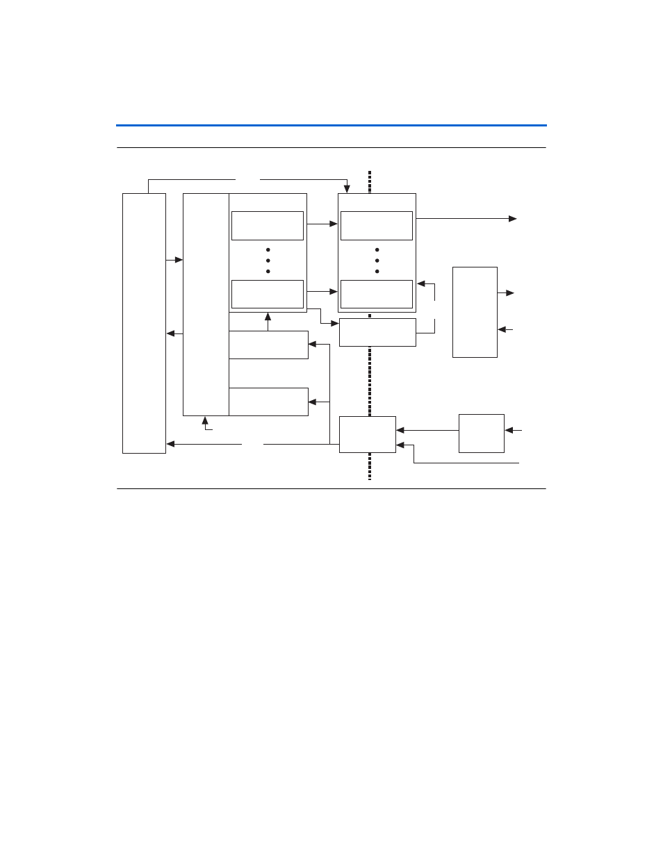
Figure 7–9. Avalon-to-PCI Block Diagram
Avalon-to-PCI Write Requests
For write requests from the interconnect, the write request is pushed on
to the PCI bus as a configuration write, I/O write, or memory write.
When the Avalon-to-PCI command/write data buffer either has enough
data to complete the full burst or 8 data phases (32 bytes on a 32-bit PCI
bus or 64 bytes on a 64-bit bus) are exceeded, the PCI master controller
will issue the PCI write transaction.
The PCI write is issued to configuration, I/O, or memory space based on
the address translation table. Refer to
.
For all PCI memory write commands, a linear incrementing burst order
is used.
Pending Read
Pending Read N
Control/Address
Pending Read 0
Control/Address
Current Write
Control/Address
PCI
Master
Command
Arbiter/
Controller
PCI
MegaCore
Function
Resp Buffer
Resp Buffer
Read Control
Command/
Data Buffer
Resp Buffer N
Avalon
Interface
Control
Logic
Addr
Translation
Control
Read
Data
Data
Read/Write
Write
Data
Addr
I/O and Cfg Requests
PCI Clock Domain Avalon Clock Domain
PCI Bus Access
Avalon Slave
Control
Resp Buffer 0
Data
Wr
Addr
Rd
Wr
Wr
Addr
Read
Addr
Bypassable
Read Cmd Buffer