Altera PHYLite User Manual
Page 22
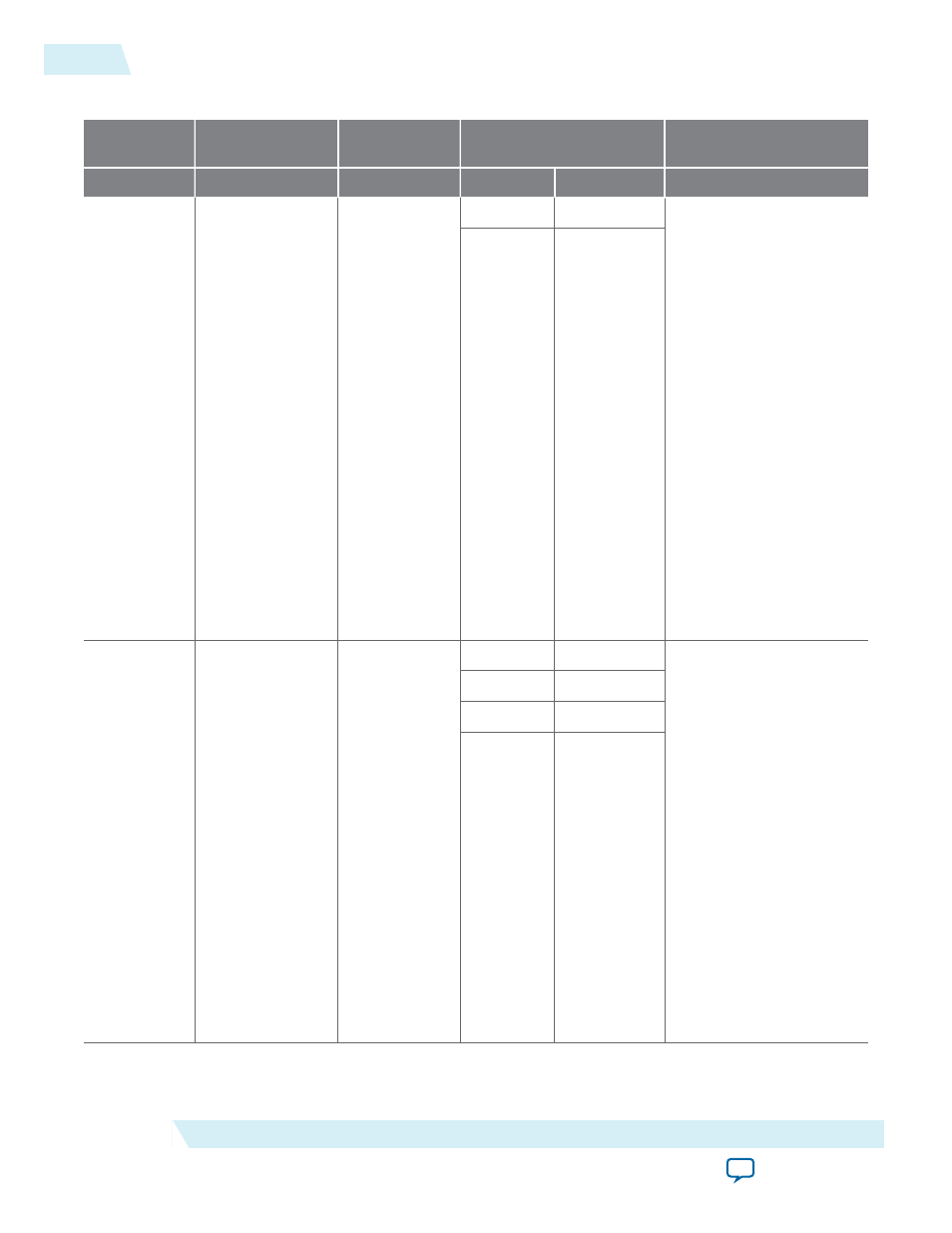
Table 11: Address Map
Feature
Avalon Address R/
W
Address CSR R
Control
Value
Field
Range
Pin Output
Phase
{id[3:0],
3'h2,lane_
addr[7:0],pin{4
:0],8'D0}
{id[3:0],
3'h1,lane_
addr[7:0],pi
n{4:0],8'E8}
Phase Value
12..0
Minimum Setting: Refer
Maximum Setting: Refer
Incremental Delay: 1/
128th VCO clock period
Note:
The pin
output phase
switches
from the CSR
value to the
Avalon value
after the first
Avalon write.
It is only
reset to the
CSR value on
a reset of the
interface.
Reserved
31..13
Pin PVT
Compensa
ted Input
Delay
{id[3:0],
3'h2,lane_
addr[7:0],
4'hC,lgc_
sel[1:0],pin_
off[2:0],4'h0}
• lgc_sel[1:0] is:
• 2'b01 for pin
<=5
• 2'b10 for pin
> 5
• pin_off[2:0] is:
• pin[2:0] for
pin <= 5
• pin[2:0] -
3'h6 for pin
> 5
Not supported
Delay Value
8..0
Minimum Setting: 0
Maximum Setting: 511
VCO clock periods
Incremental Delay: 1/
256th VCO clock period
Reserved
11..9
Enable
12
Reserved
31..13
22
Addressing
ug_altera_phylite
2015.01.16
Altera Corporation
Altera PHYLite for Parallel Interfaces IP Core User Guide