Input path – Altera PHYLite User Manual
Page 8
Advertising
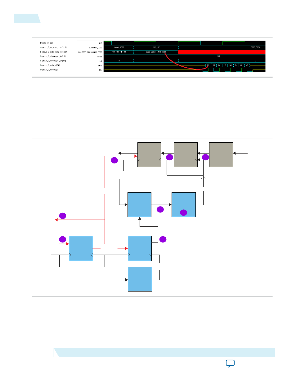
Figure 8: Example Output for Quarter Rate DDR
Related Information
•
For more information about the AFI 3.0 specification
Input Path
Figure 9: Input Path
This figure shows the input path of the IP core.
Read FIFO
DDIO
Delay Chain
(PVT)
data_to_core
data_in
phy_clk
strobe_in
dqs
Delay Chain
(PVT)
dqs_clean
pstamble_reg
FIFO
Interpolator
interpolator_clk
dqs_enable
phy_clk_phs
VFIFO
read_enable
dqs_enable
rdata_en
phy_clk
rdata_valid
data_io
strobe_io
strobe_in_n
6
1
2
3
4
5
5
6
The input path of the IP core consists of a data path, a strobe path, and read enable path.
8
Input Path
ug_altera_phylite
2015.01.16
Altera Corporation
Altera PHYLite for Parallel Interfaces IP Core User Guide
Advertising