Output path data alignment – Altera PHYLite User Manual
Page 7
Advertising
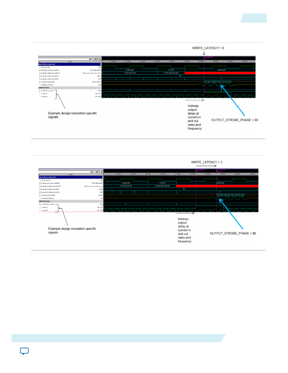
Figure 6: Output Path - Write Latency 0
These figures show the waveform diagrams for the output path.
Figure 7: Output Path - Write Latency 3
Related Information
For more information about output path signals
Output Path Data Alignment
The
data_from_core
and
oe_from_core
signals are arranged in time slices, which are broken down into
the individual pins in the group. The first time slice is on the LSBs of the busses, which matches the Altera
PHY interface (AFI) bus ordering of the Arria 10 External Memory Interfaces IP core.
{...,time2,time1,time0}
Where
time0
=
{...,pin1,pin0}
ug_altera_phylite
2015.01.16
Output Path Data Alignment
7
Altera PHYLite for Parallel Interfaces IP Core User Guide
Altera Corporation
Advertising