Clock frequency relationships, Vco frequency multiplication factor – Altera PHYLite User Manual
Page 4
Clock Domain
Description
Core clock
This clock is generated internally by the IP core and output to the core to be used for
all transfers between the FPGA core and the IP core.
PHY Clock
This clock is used internally by the IP core for PHY circuitry running at the same
frequency as the core clock. The PHY circuitry ensures that this clock is kept in phase
with the core clock for core-to-periphery and periphery-to-core transfers.
VCO clock
This clock is generated internally by the PLL. It is used by both the input and output
paths to generate PVT compensated delays.
External Memory
Clock
This is the user specified frequency at which the FPGA I/Os connected to the
external device operate.
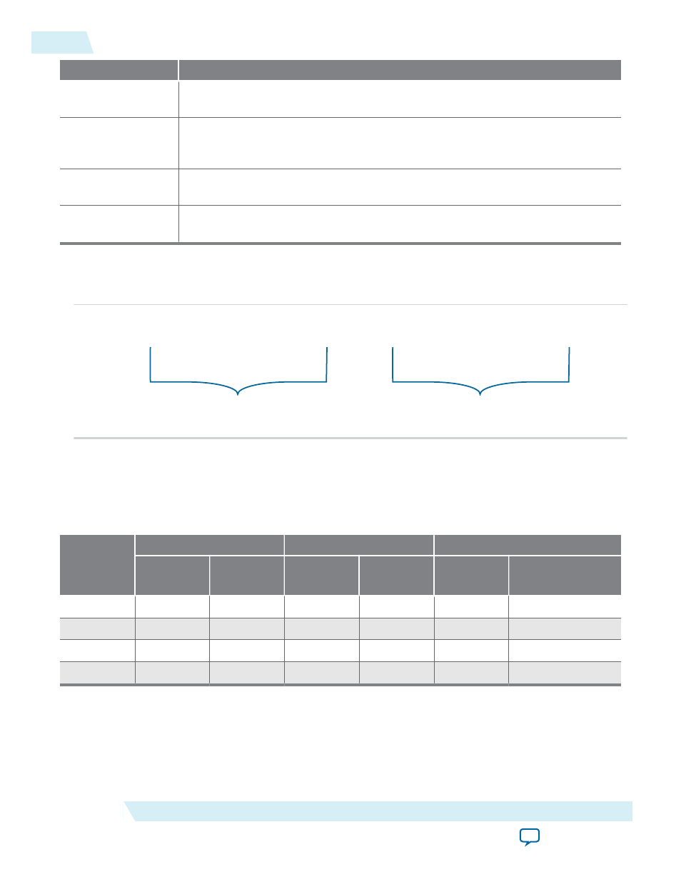
Clock Frequency Relationships
Figure 3: Clock Frequency Relationships
VCO Clock Frequency : External Memory Clock Frequency : Core/PHY Clock Frequency
VCO Frequency Multiplier
User Specified Core Clock Rate
VCO Frequency Multiplication Factor
The relationship between the VCO clock frequency and the user specified external memory clock
frequency is calculated during generation of the IP core based on the this table.
Table 1: VCO Frequency Multiplication Factor
VCO
Frequency
Multiplication
Factor
Speed Grade -1
Speed Grade -2
Speed Grade -3
Minimum
Frequency
Maximum
Frequency
Minimum
Frequency
Maximum
Frequency
Minimum
Frequency
Maximum Frequency
1
600
800
600
800
550
800
2
300
600
300
600
275
550
4
150
300
150
300
137.5
275
8
100
150
100
150
100
137.5
4
Clock Frequency Relationships
ug_altera_phylite
2015.01.16
Altera Corporation
Altera PHYLite for Parallel Interfaces IP Core User Guide