Altera PHYLite User Manual
Page 30
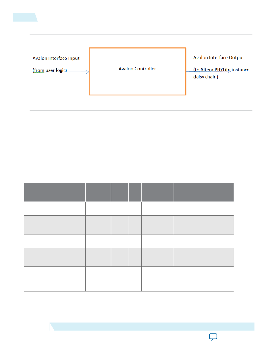
Figure 18: Avalon Controller
The input interface is as follows:
avl_in_address[31:0]
=
{8'h00,interface_id[3:0],grp[4:0],pin[5:0],csr[0],register[7:0]}
Note: There is no look-up stage here. All necessary data is automatically looked-up and
cached by the Avalon controller.
Note: A single controller can support multiple interfaces in an I/O column.
Table 15: Avalon Controller Registers
This table lists the available registers in the Avalon controller. For more information, refer to
.
Register[7:0]
Pin[5:0]
Csr[0] Aval
on
R/W
CSR R/W
R/W Data on avl_readdata/
avl_writedata
AVL_CTRL_REG_
NUM_GROUPS
0
0
R
N/A
{24'h000000,num_
grps[7:0]}
AVL_CTRL_REG_
GROUP_INFO
0
0
R
N/A
{16'h0000,num_
lanes[7:0],num_
pins[7:0]}
AVL_CTRL_REG_
IDELAY
0-47
0
R/W
N/A
{23'h000000,dq_
delay[8:0]}
AVL_CTRL_REG_
ODELAY
0-47
R: 0/1
W: 0
R/W
R
{19'h00000,output_
phase[12:0]}
AVL_CTRL_REG_DQS_
DELAY
0: DQS A
1: DQS B
(6)
0
R/W
N/A
{22'h000000,dqs_
delay[9:0]}
(6)
Strobe logic B is only used by the negative pin of complementary strobes
30
Example Design Avalon Controller
ug_altera_phylite
2015.01.16
Altera Corporation
Altera PHYLite for Parallel Interfaces IP Core User Guide