Altera PHYLite User Manual
Page 48
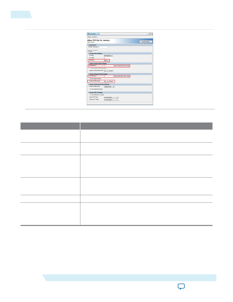
Figure 23: Additional Parameter in Group Tab
Table 24: Additional Parameters in the Altera PHYLite for Parallel Interfaces IP Core
Parameter
Description
PLL reference clock frequency Because PLL is available in each I/O bank, you only need to specify the
reference clock frequency for the PLL. No PLL instantiation is required.
Clock rate of user logic
The setting (full/half/quarter) is applicable for all groups in the IP core. In
the ALTDQ_DQS2 IP core, only full and half rate are supported.
DDR/SDR
This setting is applicable to the respective group only. In the ALTDQ_
DQS2 IP core, the default setting is DDR. For Altera PHYLite for Parallel
Interfaces IP core, if you need to implement SDR, then in the DDR/SDR
parameter, select SDR.
Read latency
The latency between a read command sent to the external device and the
first read data returned to the FPGA. This feature internally controls the
strobe enable gating.
Write Latency
This is the latency between the write command and the first written data.
Output Strobe Phase
Enables you to set the phase shift between the output strobe and output
data. In the ALTDQ_DQS2 IP core, you must ensure phase shifts by
generating two clocks with different phases, or manipulating some
dynamic reconfiguration settings.
48
Additional Parameter for the Altera PHYLite for Parallel Interfaces IP core
ug_altera_phylite
2015.01.16
Altera Corporation
Altera PHYLite for Parallel Interfaces IP Core User Guide