Altera Stratix V Advanced Systems Development Board User Manual
Page 13
Chapter 2: Board Components
2–3
Board Overview
January 2014
Altera Corporation
Stratix V Advanced Systems Development Board
Reference Manual
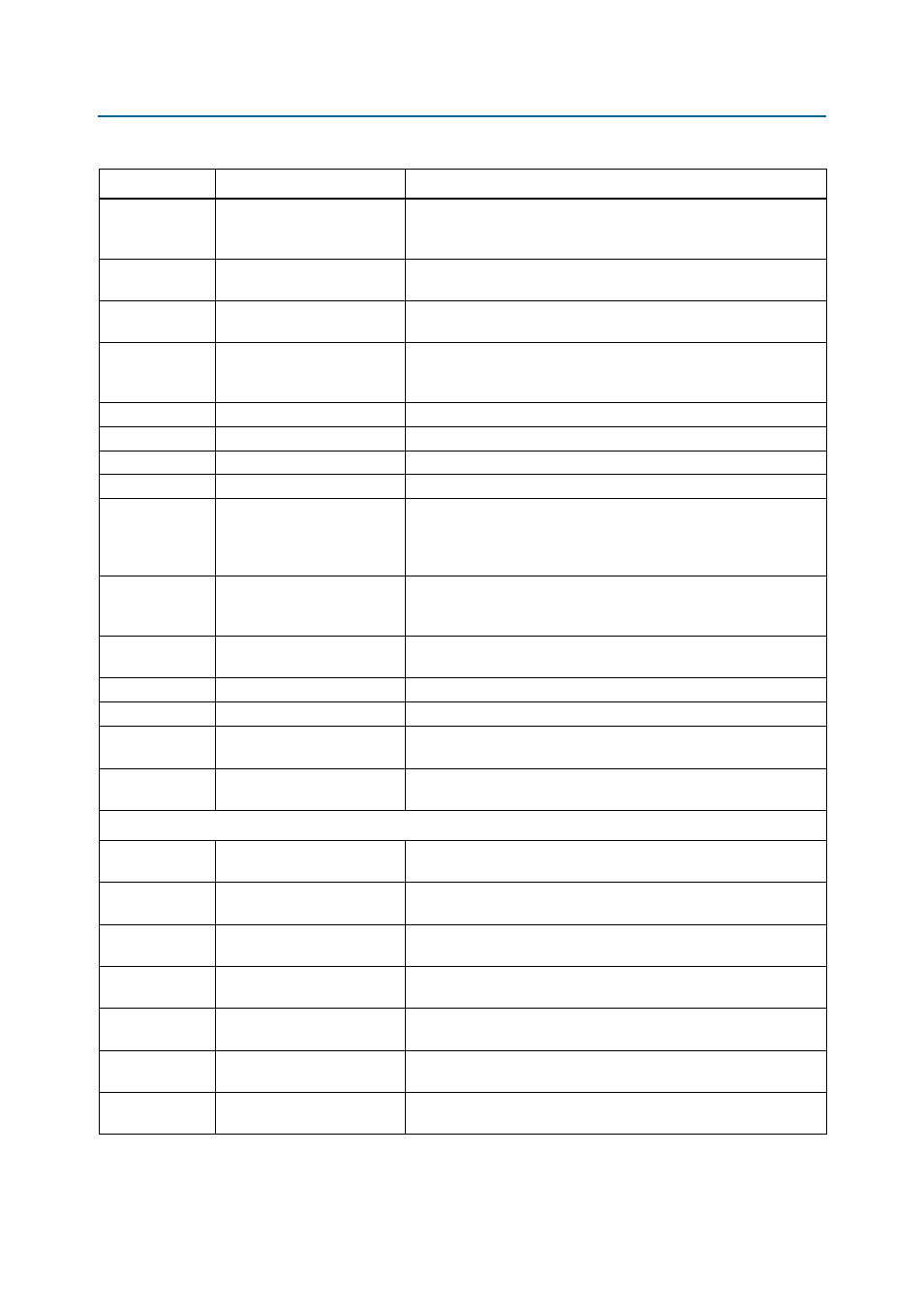
SW8
PCI Express DIP switch
Controls the PCI Express lane width by connecting the prsnt pins
together on the PCI Express edge connector. This switch is located at
the back of the board.
S1
Program select push button
Toggles the program LEDs, which selects the program image that
loads from flash memory to the FPGAs.
S2
Program configuration push
button
Configures the FPGAs from flash memory image based on the program
LEDs.
D1, D2, D3
Program LEDs
Illuminates to show the LED sequence that determines which flash
memory image loads to the FPGA when you press the program select
push button.
D12
Load LED
Illuminates during FPGA configuration.
D13
Configuration done LED
Illuminates when the FPGA is configured.
D14
Error LED
Illuminates when the FPGA configuration from flash fails.
D27
Power LED
Illuminates when 5-V power is present.
D4, D5
System Console TX/RX LEDs
Indicate the transmit or receive activity of the System Console USB
interface. The TX and RX LEDs would flicker if the link is in use and
active. The LEDs are either off when not in use or on when in use but
idle.
D15, D16
JTAG TX/RX LEDs
Indicate the transmit or receive activity of the JTAG chain. The TX and
RX LEDs would flicker if the link is in use and active. The LEDs are
either off when not in use or on when in use but idle.
D10, D11
HSMC TX/RX LEDs
You can configure these LEDs to indicate transmit or receive activity on
the HSMC interface.
D21
HSMC Present LED
Illuminates when you plug a daughtercard into the HSMC connector.
D36
FMC Present LED
Illuminates when you plug a daughtercard into the FMC connector.
D42, D43
PCI Express Gen2/Gen3 LED
You can configure these LEDs to illuminate when PCI Express is in
Gen2 or Gen3 mode.
D38, D39, D40,
D41
PCI Express Link LEDs
You can configure these LEDs to display the PCI Express link width
(x1, x4, x8, x16).
Clock Circuitry
X1
125 M oscillator
125.000-MHz crystal oscillator for general purpose logic. A buffered
copy of this clock is available on FPGA1 and FPGA2.
X2
50 M oscillator
50.000-MHz crystal oscillator for general purpose logic. A buffered
copy of this clock is available on FPGA1, FPGA2, and MAX V CPLD.
U53
Quad-output oscillator
Programmable oscillator with default LVDS frequencies of 625 MHz,
206.25 MHz, 625 MHz, and 206.25 MHz.
U82
Quad-output oscillator
Programmable oscillator with default frequencies of 100 MHz (LVDS),
100 MHz (LVDS), 100 MHz (1.8-V CMOS), and 100 MHz (LVDS).
U95
Quad-output oscillator
Programmable oscillator with default LVDS frequencies of 100 MHz,
706.25 MHz, 206.25 MHz, and 206.25 MHz.
U100
Quad-output oscillator
Programmable oscillator with default frequencies of 100 MHz (LVDS),
100 MHz (LVDS), 100 MHz (1.8-V CMOS), and 100 MHz (LVDS).
X91
Quad-output oscillator
Programmable oscillator with default LVDS frequencies of 100 MHz,
644.53125 MHz, 644.53125 MHz, and 100 MHz.
Table 2–1. Stratix V Advanced Systems Development Board Components (Part 2 of 4)
Board Reference
Type
Description