General user input/output, User-defined push buttons, User-defined dip switches – Altera Stratix V Advanced Systems Development Board User Manual
Page 36: General user input/output –26
2–26
Chapter 2: Board Components
General User Input/Output
Stratix V Advanced Systems Development Board
January 2014
Altera Corporation
Reference Manual
General User Input/Output
This section describes the user I/O interface to the FPGAs. This section describes the
following I/O elements:
■
User-defined push buttons
■
User-defined DIP switches
■
User-defined LEDs
User-Defined Push Buttons
The development board includes three user-defined push buttons for each FPGA
device. Board references S4, S5, and S6 are push buttons that allow you to interact
with the FPGA1 device while S8, S9, and S10 are to interact with the FPGA2 device.
When you press and hold down the push button, the device pin is set to logic 0; when
you release the push button, the device pin is set to logic 1. There is no board-specific
function for these general user push buttons.
Table 2–15
lists the user-defined push button schematic signal names and their
corresponding Stratix V GX FPGA device pin numbers.
User-Defined DIP Switches
Board reference SW1 and SW3 are two sets of eight-pin DIP switch, one switch for
each FPGA. The switches are user-defined, and are for additional FPGA input control.
When the switch is in the CLOSED or ON position, a logic 0 is selected. When the
switch is in the OPEN or OFF position, a logic 1 is selected. There is no board-specific
function for these switches.
Table 2–16
lists the user-defined DIP switch schematic signal names and their
corresponding Stratix V GX FPGA pin numbers.
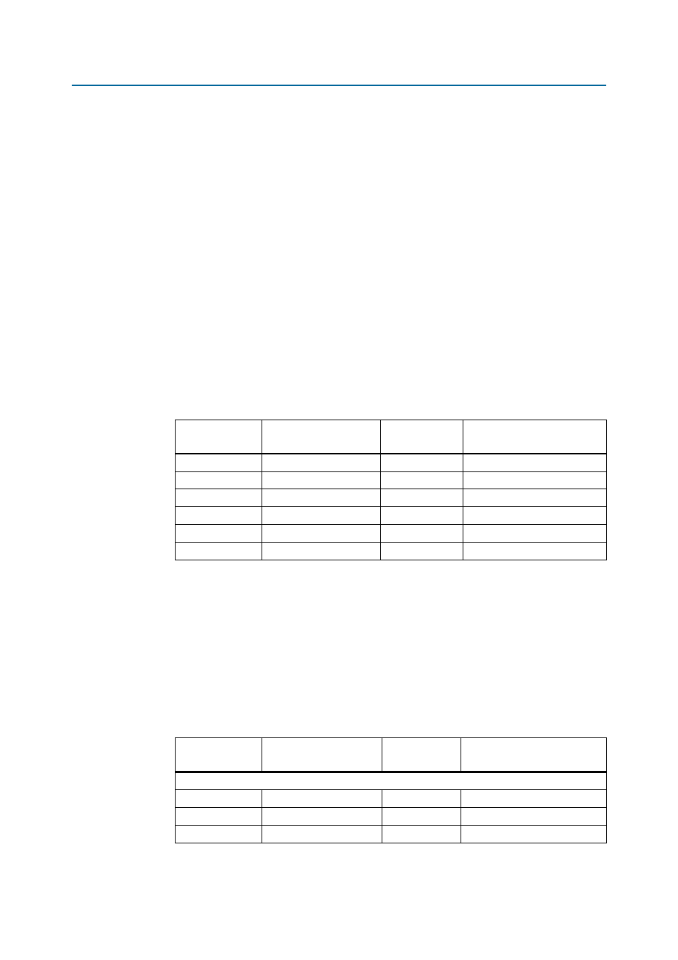
Table 2–15. User-Defined Push Button Schematic Signal Names and Functions
Board Reference
Schematic Signal Name
I/O Standard
Stratix V GX FPGA Device Pin
Number
S4
FPGA1_PB2
1.5-V
BA34
S5
FPGA1_PB1
1.5-V
BA33
S6
FPGA1_PB0
1.5-V
AY33
S8
FPGA2_PB2
1.5-V
U26
S9
FPGA2_PB1
1.5-V
U27
S10
FPGA2_PB0
1.5-V
V26
Table 2–16. User-Defined DIP Switch Schematic Signal Names and Functions (Part 1 of 2)
Board Reference
Schematic Signal Name
I/O Standard
Stratix V GX FPGA Device Pin
Number
FPGA1 User DIP Switch (SW1)
1
FPGA1_DIPSW0
1.5-V
V26
2
FPGA1_DIPSW1
1.5-V
V27
3
FPGA1_DIPSW2
1.5-V
AH22