Altera Stratix V Advanced Systems Development Board User Manual
Page 24
2–14
Chapter 2: Board Components
Configuration, Status, and Setup Elements
Stratix V Advanced Systems Development Board
January 2014
Altera Corporation
Reference Manual
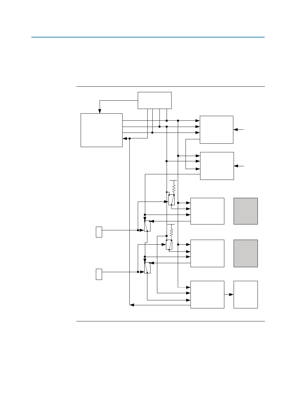
JTAG Chain
The on-board USB-Blaster II is automatically disabled when you connect an external
USB-Blaster to the JTAG chain or when you enable JTAG from the PCI Express edge
connector.
illustrates the JTAG chain.
Each jumper shown in
is located in the JTAG DIP switch (SW7) on the back
of the board. Both the Stratix V FPGAs and the MAX VSystem Controller are always
in the JTAG chain. To connect the HSMC or FMC interface in the chain, their
corresponding switch must be in the OFF position.
Figure 2–3. JTAG Chain
GPIO
Cypress
On-Board
USB-Blaster II
Analog
Switch
5M2210
System
Controller
FMC
HSMC
GPIO
GPIO
GPIO
JTAG Master
GPIO
DISABLE
JTAG Slave
JTAG Slave
Installed
HSMC
Card
Installed
FMC
Card
Flash
Memory
TCK
TMS
TDI
TDO
TCK
TMS
TDI
TDO
TCK
TMS
TDI
TDO
TCK
TMS
TDI
TDO
JTAG Slave
JTAG Slave
5SGXA7
FPGA1
5SGXA7
FPGA2
Analog
Switch
ENABLE
ENABLE
ALWAYS
ENABLED
(in chain)
ALWAYS
ENABLED
(in chain)
DIP Switch
DIP Switch
10-pin
JTAG Header
TCK
TMS
TDI
TDO
JTAG Slave
TCK
TMS
TDO
TDI
2.5 V
2.5 V