Altera Stratix V Advanced Systems Development Board User Manual
Page 63
Chapter 2: Board Components
2–53
Memory
January 2014
Altera Corporation
Stratix V Advanced Systems Development Board
Reference Manual
A3
DQ63
1.5-V SSTL Class I
BB29
C13
Data bus
F3
DQS_P0
Differential 1.5-V
SSTL Class I
AY30
D21
Data strobe
G3
DQS_N0
Differential 1.5-V
SSTL Class I
BA29
D20
Data strobe
C7
DQS_P1
Differential 1.5-V
SSTL Class I
AE27
H21
Data strobe
B7
DQS_N1
Differential 1.5-V
SSTL Class I
AE28
H20
Data strobe
F3
DQS_P2
Differential 1.5-V
SSTL Class I
AL30
V21
Data strobe
G3
DQS_N2
Differential 1.5-V
SSTL Class I
AL31
V20
Data strobe
C7
DQS_P3
Differential 1.5-V
SSTL Class I
AJ25
T20
Data strobe
B7
DQS_N3
Differential 1.5-V
SSTL Class I
AJ26
T19
Data strobe
F3
DQS_P4
Differential 1.5-V
SSTL Class I
AR27
L15
Data strobe
G3
DQS_N4
Differential 1.5-V
SSTL Class I
AR28
K14
Data strobe
C7
DQS_P5
Differential 1.5-V
SSTL Class I
AK30
V17
Data strobe
B7
DQS_N5
Differential 1.5-V
SSTL Class I
AL29
U17
Data strobe
F3
DQS_P6
Differential 1.5-V
SSTL Class I
AT26
Y16
Data strobe
G3
DQS_N6
Differential 1.5-V
SSTL Class I
AU26
W16
Data strobe
C7
DQS_P7
Differential 1.5-V
SSTL Class I
BC28
E15
Data strobe
B7
DQS_N7
Differential 1.5-V
SSTL Class I
BD28
D15
Data strobe
K1
ODT
1.5-V SSTL Class I
AF34
L18
On-die termination enable
J3
RASN
1.5-V SSTL Class I
AN33
J19
Row address strobe
T2
RESETN
1.5-V SSTL Class I
AE30
R19
Reset
L3
WEN
1.5-V SSTL Class I
AP33
H16
Write enable
L8
ZQ01
—
—
—
ZQ impedance calibration
L8
ZQ02
—
—
—
ZQ impedance calibration
L8
ZQ03
—
—
—
ZQ impedance calibration
L8
ZQ04
—
—
—
ZQ impedance calibration
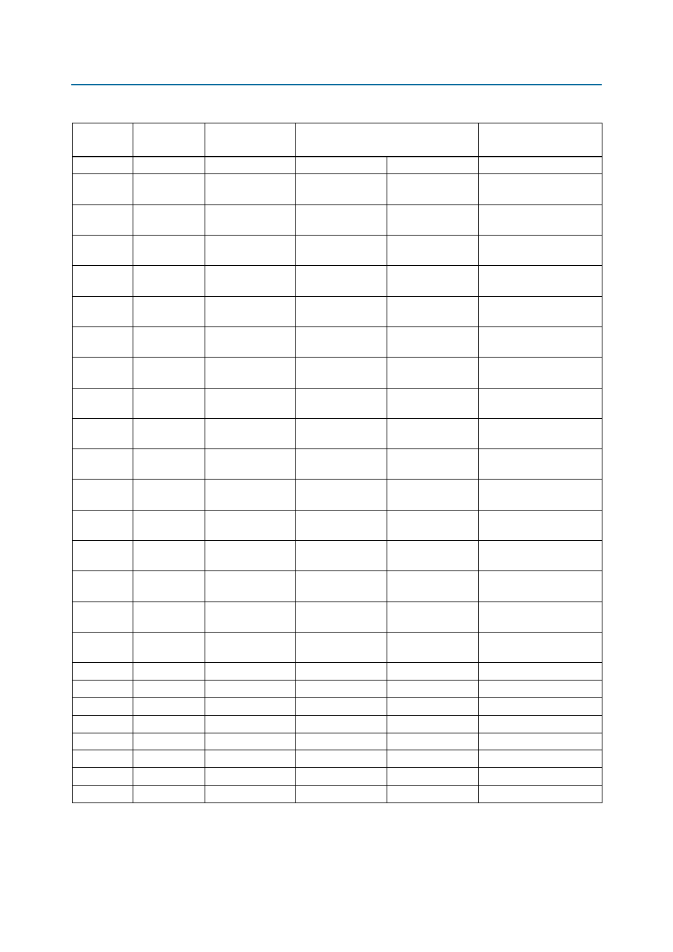
Table 2–24. FPGA2 DDR3 Devices Pin Assignments, Schematic Signal Names, and Functions (Part 6 of 6)
Board
Reference
Schematic
Signal Name
I/O Standard
Stratix V GX FPGA2 Device Pin Number
Description