Altera Stratix V Advanced Systems Development Board User Manual
Page 72
2–62
Chapter 2: Board Components
Memory
Stratix V Advanced Systems Development Board
January 2014
Altera Corporation
Reference Manual
AA21
MOSYS2_QATX_P0
1.4-V PCML
AK2
Transceiver input
W20
MOSYS2_QATX_P1
1.4-V PCML
AH2
Transceiver input
AA19
MOSYS2_QATX_P2
1.4-V PCML
AF2
Transceiver input
W18
MOSYS2_QATX_P3
1.4-V PCML
AD2
Transceiver input
AA17
MOSYS2_QATX_P4
1.4-V PCML
AB2
Transceiver input
W16
MOSYS2_QATX_P5
1.4-V PCML
Y2
Transceiver input
AA15
MOSYS2_QATX_P6
1.4-V PCML
V2
Transceiver input
W14
MOSYS2_QATX_P7
1.4-V PCML
T2
Transceiver input
AB11
MOSYS2_QBTX_N0
1.4-V PCML
P1
Transceiver input
Y10
MOSYS2_QBTX_N1
1.4-V PCML
M1
Transceiver input
AB9
MOSYS2_QBTX_N2
1.4-V PCML
K1
Transceiver input
Y8
MOSYS2_QBTX_N3
1.4-V PCML
H1
Transceiver input
AB7
MOSYS2_QBTX_N4
1.4-V PCML
F1
Transceiver input
Y6
MOSYS2_QBTX_N5
1.4-V PCML
B1
Transceiver input
AB5
MOSYS2_QBTX_N6
1.4-V PCML
D1
Transceiver input
Y4
MOSYS2_QBTX_N7
1.4-V PCML
C3
Transceiver input
AA11
MOSYS2_QBTX_P0
1.4-V PCML
P2
Transceiver input
W10
MOSYS2_QBTX_P1
1.4-V PCML
M2
Transceiver input
AA9
MOSYS2_QBTX_P2
1.4-V PCML
K2
Transceiver input
W8
MOSYS2_QBTX_P3
1.4-V PCML
H2
Transceiver input
AA7
MOSYS2_QBTX_P4
1.4-V PCML
F2
Transceiver input
W6
MOSYS2_QBTX_P5
1.4-V PCML
B2
Transceiver input
AA5
MOSYS2_QBTX_P6
1.4-V PCML
D2
Transceiver input
W4
MOSYS2_QBTX_P7
1.4-V PCML
C4
Transceiver input
F21
MOSYS2_RBIAS_0N
1.5-V CMOS
—
Calibration resistor
E21
MOSYS2_RBIAS_0P
1.5-V CMOS
—
Calibration resistor
F1
MOSYS2_RBIAS_1N
1.5-V CMOS
—
Calibration resistor
E1
MOSYS2_RBIAS_1P
1.5-V CMOS
—
Calibration resistor
M20
MOSYS2_READYN
1.5-V CMOS
K15
Device ready
Y22
MOSYS2_REFCLK_N
LVDS
—
Input reference clock
W22
MOSYS2_REFCLK_P
LVDS
—
Input reference clock
M22
MOSYS2_RESETN_IN
1.5-V CMOS
R15
Active low reset
P1
MOSYS2_SPI_SCLK
1.5-V CMOS
D17
SPI slave clock
T1
MOSYS2_SPI_SDI
1.5-V CMOS
C19
SPI data in
R2
MOSYS2_SPI_SDO
1.5-V CMOS
F19
SPI data out
U2
MOSYS2_SPI_SS
1.5-V CMOS
G19
SPI slave select
H9
MOSYS2_VDD_KELVIN
1.0-V
—
VDD monitor point
H8
MOSYS2_VSS_KELVIN
GND
—
VSS monitor point
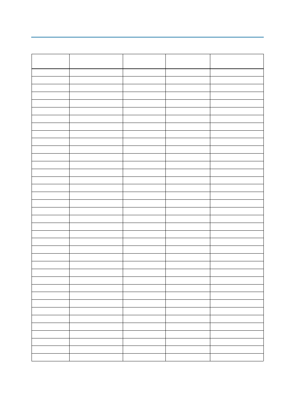
Table 2–27. MoSys MSR576 Interface Pin Assignments, Signal Names and Functions (Part 5 of 5)
Board Reference
Schematic Signal Name
I/O Standard
Stratix V GX FPGA
Device Pin Number
Description