Altera Stratix V Advanced Systems Development Board User Manual
Page 42
2–32
Chapter 2: Board Components
Components and Interfaces
Stratix V Advanced Systems Development Board
January 2014
Altera Corporation
Reference Manual
U47.A17
PCIE_RX_N3
1.4-V PCML
AY44
—
Receive data bus from PLX switch
U47.A19
PCIE_RX_N4
1.4-V PCML
AT44
—
Receive data bus from PLX switch
U47.A20
PCIE_RX_N5
1.4-V PCML
AP44
—
Receive data bus from PLX switch
U47.A22
PCIE_RX_N6
1.4-V PCML
AM44
—
Receive data bus from PLX switch
U47.A23
PCIE_RX_N7
1.4-V PCML
AK44
—
Receive data bus from PLX switch
U47.B13
PCIE_RX_P0
1.4-V PCML
BB43
—
Receive data bus from PLX switch
U47.B14
PCIE_RX_P1
1.4-V PCML
BA41
—
Receive data bus from PLX switch
U47.B16
PCIE_RX_P2
1.4-V PCML
AW41
—
Receive data bus from PLX switch
U47.B17
PCIE_RX_P3
1.4-V PCML
AY43
—
Receive data bus from PLX switch
U47.B19
PCIE_RX_P4
1.4-V PCML
AT43
—
Receive data bus from PLX switch
U47.B20
PCIE_RX_P5
1.4-V PCML
AP43
—
Receive data bus from PLX switch
U47.B22
PCIE_RX_P6
1.4-V PCML
AM43
—
Receive data bus from PLX switch
U47.B23
PCIE_RX_P7
1.4-V PCML
AK43
—
Receive data bus from PLX switch
U47.D13
PCIE_TX_N0
1.4-V PCML
AY40
—
Transmit data bus to PLX switch
U47.D14
PCIE_TX_N1
1.4-V PCML
AV40
—
Transmit data bus to PLX switch
U47.D16
PCIE_TX_N2
1.4-V PCML
AT40
—
Transmit data bus to PLX switch
U47.D17
PCIE_TX_N3
1.4-V PCML
AU42
—
Transmit data bus to PLX switch
U47.D19
PCIE_TX_N4
1.4-V PCML
AN42
—
Transmit data bus to PLX switch
U47.D20
PCIE_TX_N5
1.4-V PCML
AL42
—
Transmit data bus to PLX switch
U47.D22
PCIE_TX_N6
1.4-V PCML
AJ42
—
Transmit data bus to PLX switch
U47.D23
PCIE_TX_N7
1.4-V PCML
AG42
—
Transmit data bus to PLX switch
U47.E13
PCIE_TX_P0
1.4-V PCML
AY39
—
Transmit data bus to PLX switch
U47.E14
PCIE_TX_P1
1.4-V PCML
AV39
—
Transmit data bus to PLX switch
U47.E16
PCIE_TX_P2
1.4-V PCML
AT39
—
Transmit data bus to PLX switch
U47.E17
PCIE_TX_P3
1.4-V PCML
AU41
—
Transmit data bus to PLX switch
U47.E19
PCIE_TX_P4
1.4-V PCML
AN41
—
Transmit data bus to PLX switch
U47.E20
PCIE_TX_P5
1.4-V PCML
AL41
—
Transmit data bus to PLX switch
U47.E22
PCIE_TX_P6
1.4-V PCML
AJ41
—
Transmit data bus to PLX switch
U47.E23
PCIE_TX_P7
1.4-V PCML
AG41
—
Transmit data bus to PLX switch
U47.H23
PCIE_RX_N8
1.4-V PCML
—
BB44
Receive data bus from PLX switch
U47.J23
PCIE_RX_N9
1.4-V PCML
—
BA42
Receive data bus from PLX switch
U47.L23
PCIE_RX_N10
1.4-V PCML
—
AW42
Receive data bus from PLX switch
U47.M23
PCIE_RX_N11
1.4-V PCML
—
AY44
Receive data bus from PLX switch
U47.P23
PCIE_RX_N12
1.4-V PCML
—
AT44
Receive data bus from PLX switch
U47.R23
PCIE_RX_N13
1.4-V PCML
—
AP44
Receive data bus from PLX switch
U47.U23
PCIE_RX_N14
1.4-V PCML
—
AM44
Receive data bus from PLX switch
U47.V23
PCIE_RX_N15
1.4-V PCML
—
AK44
Receive data bus from PLX switch
U47.H22
PCIE_RX_P8
1.4-V PCML
—
BB43
Receive data bus from PLX switch
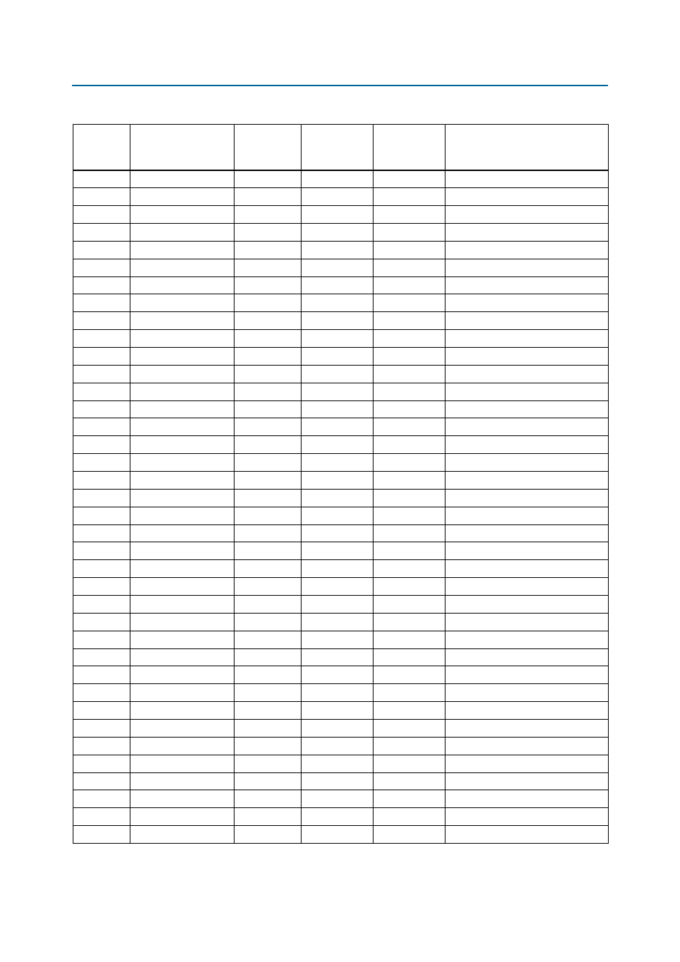
Table 2–20. PCI Express Pin Assignments, Schematic Signal Names, and Functions (Part 2 of 3)
Board
Reference
(J13)
Schematic Signal
Name
I/O Standard
Stratix V GX
FPGA1 Device
Pin Number
Stratix V GX
FPGA2 Device
Pin Number
Description