Fpga programming from cfi flash memory, Fpga programming from cfi flash memory –16 – Altera Stratix V Advanced Systems Development Board User Manual
Page 26
2–16
Chapter 2: Board Components
Configuration, Status, and Setup Elements
Stratix V Advanced Systems Development Board
January 2014
Altera Corporation
Reference Manual
FPGA Programming from CFI Flash Memory
On either board power-up or by pressing the program load push button (S2), the
MAX V CPLD System Controller’s parallel flash loader configures the FPGA from the
flash memory. The system controller uses the Altera Parallel Flash Loader (PFL)
megafunction which reads 16-bit data from the flash memory and converts it to fast
passive parallel (FPP) format. This 16-bit data is then written to the FPGA’s dedicated
configuration pins during configuration.
After a board power-up or reset event, the MAX V CPLD (U73) automatically
configures the FPGAs in FPP mode with the pre-installed factory .pof file. There are
three pages reserved for the FPGA configuration data—factory FPGA1 (page 0),
factory FPGA2 (page 1), and user design FPGA1 (page 2).
1
You must set the FPGA1_MSEL[4:0] or FPGA2_MSEL[4:0] DIP switch to FPP x8 mode
to configure FPGA1 or FPGA2 via FPP.
f
For more information about the FPP configuration mode, refe
pter in the Stratix V
Handbook.
Three green configuration status LEDs, PGM_LED[2:0] (D1, D2, D3) indicates the status
of the FPP configuration.
lists the configuration status LEDs settings.
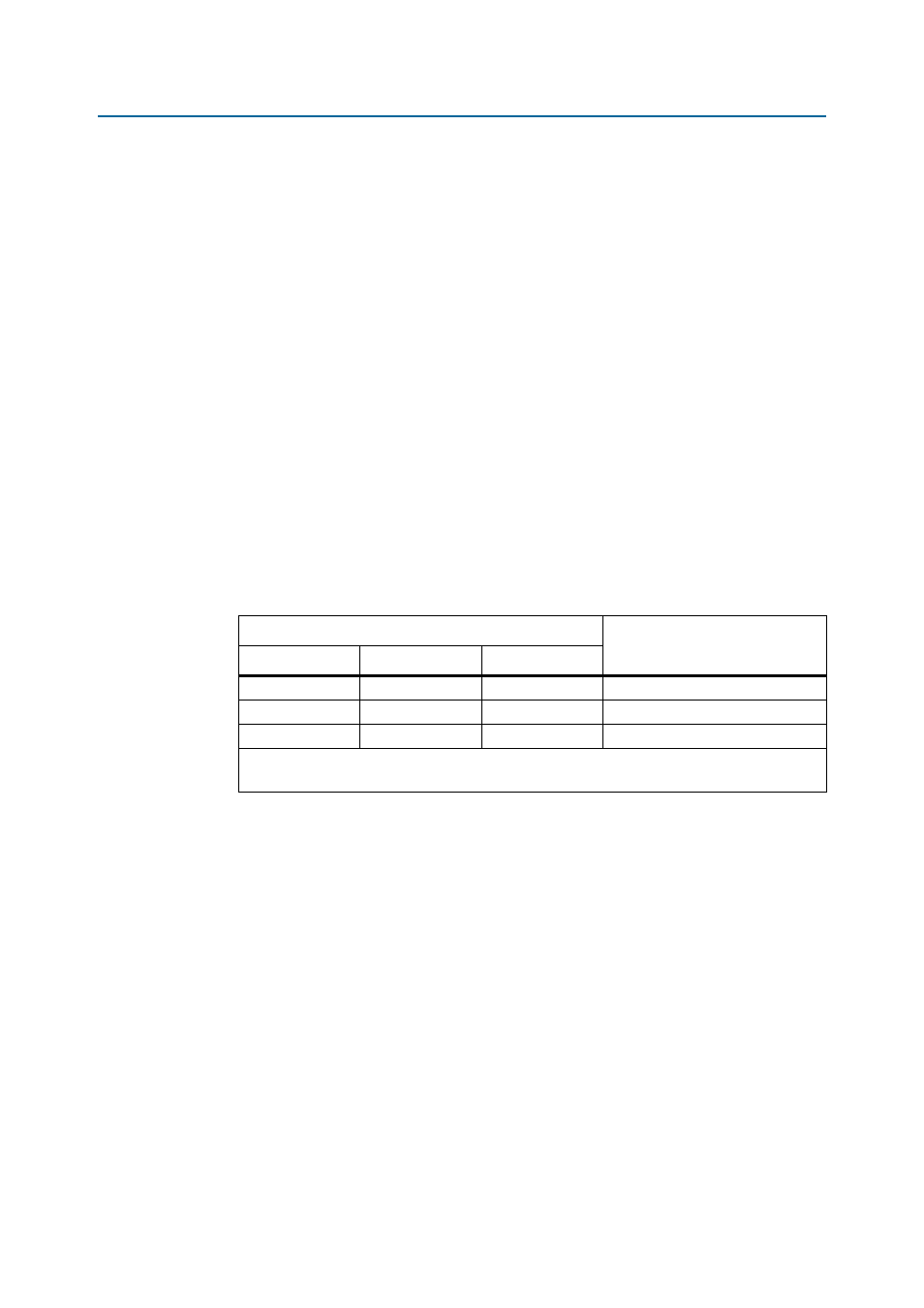
Table 2–7. Configuration LED settings
(1)
LED
Design
PGM_LED0
PGM_LED1
PGM_LED2
v
—
—
Factory FPGA1
—
v
—
Factory FPGA2
—
—
v
User design FPGA1
Note to
(1) A checkmark (
v) indicates that the LED is ON (logic 0) while a dash (—) indicates that the LED is OFF (logic 1).