Altera Stratix V Advanced Systems Development Board User Manual
Page 41
Chapter 2: Board Components
2–31
Components and Interfaces
January 2014
Altera Corporation
Stratix V Advanced Systems Development Board
Reference Manual
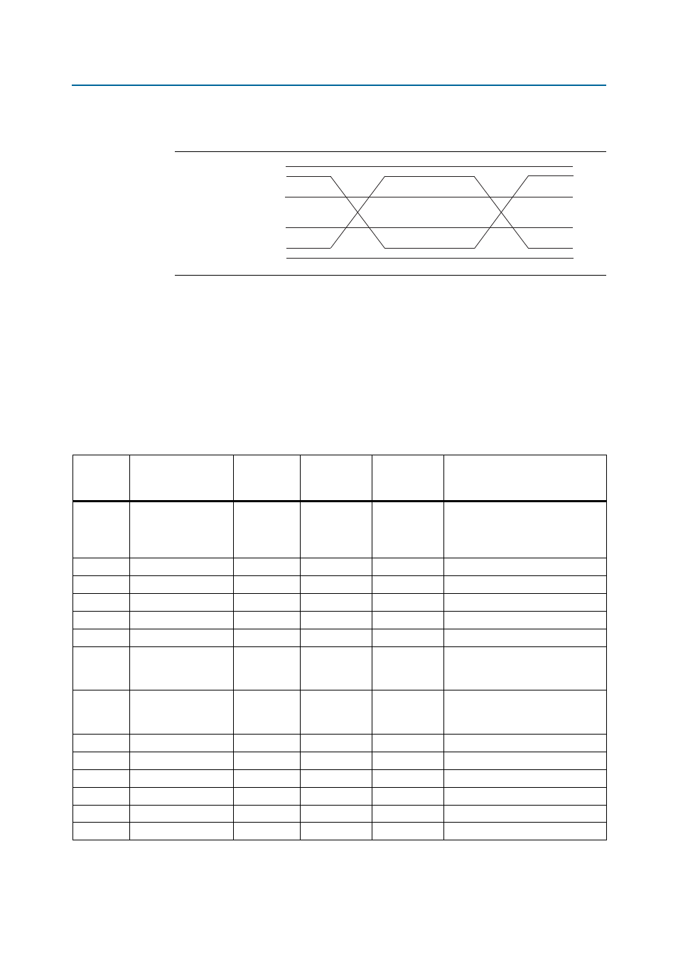
shows the PCI Express reference clock levels.
The PCI Express edge connector also has a presence detect feature for the
motherboard to determine if a card is installed. A jumper is provided to optionally
connect PRSNT1n to any of the four PRSNT2n pins found within the x16 connector
definition. This is to address issues on some PC systems that would base the
link-width capability on the presence detect pins versus a query operation. Connect
any of the four PRSNT2n pins to the PRSNT1n pin using the PCIE_PRSNTn (SW8) DIP
switch.
summarizes the PCI Express pin assignments. The signal names and
directions are relative to the Stratix V GX FPGAs.
Figure 2–6. PCI Express Reference Clock Levels
V
MAX
= 1.15 V
V
CROSS MAX
= 550 mV
V
CROSS MIN
= 250 mV
V
MIN
= –0.30 V
REFCLK –
REFCLK +
Table 2–20. PCI Express Pin Assignments, Schematic Signal Names, and Functions (Part 1 of 3)
Board
Reference
(J13)
Schematic Signal
Name
I/O Standard
Stratix V GX
FPGA1 Device
Pin Number
Stratix V GX
FPGA2 Device
Pin Number
Description
A11
PCIE_PERSTn
LVTTL
AU33
AU33
Reset, indicating that the PCI
Express main power is stable (3.3 V
to 1.8 V translator to Stratix V
devices and PEX8747).
A1
PCIE_PRSNT1n
LVTTL
—
—
Presence detect DIP switch
B17
PCIE_PRSNT2n_X1
LVTTL
—
—
Presence detect DIP switch
B31
PCIE_PRSNT2n_X4
LVTTL
—
—
Presence detect DIP switch
B48
PCIE_PRSNT2n_X8
LVTTL
—
—
Presence detect DIP switch
B81
PCIE_PRSNT2n_X16
LVTTL
—
—
Presence detect DIP switch
A14
PCIE_REFCLK_N
HCSL
AK39
AK39
Motherboard reference clock. Fan
out buffer to Stratix V devices and
PEX8747.
A13
PCIE_REFCLK_P
HCSL
AK38
AK38
Motherboard reference clock. Fan
out buffer to Stratix V devices and
PEX8747.
B5
PCIE_SMCLK
LVTTL
—
—
SMB clock (optional)
B6
PCIE_SMDAT
LVTTL
—
—
SMB address or data (optional)
B11
PCIE_WAKEn
LVTTL
—
—
Wake signal
U47.A13
PCIE_RX_N0
1.4-V PCML
BB44
—
Receive data bus from PLX switch
U47.A14
PCIE_RX_N1
1.4-V PCML
BA42
—
Receive data bus from PLX switch
U47.A16
PCIE_RX_N2
1.4-V PCML
AW42
—
Receive data bus from PLX switch