Altera Stratix V Advanced Systems Development Board User Manual
Page 35
Chapter 2: Board Components
2–25
Clock Circuitry
January 2014
Altera Corporation
Stratix V Advanced Systems Development Board
Reference Manual
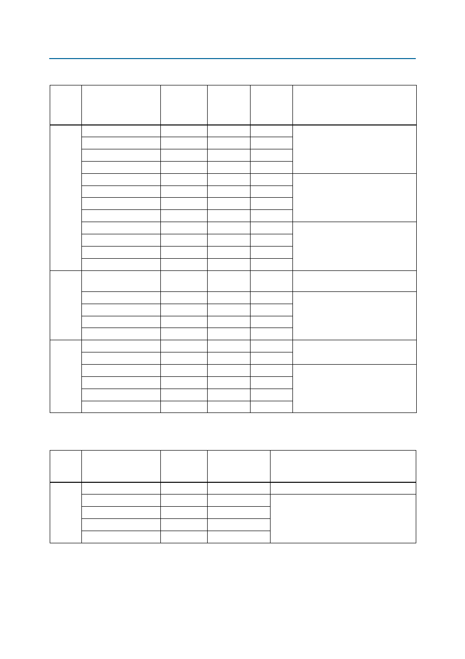
lists the clock outputs for the development board.
FMC
FMC_CLK_M2C_P[0]
LVDS
J18 —
LVDS clock input from the installed FMC
cable or board.
FMC_CLK_M2C_N[0]
LVDS
H18 —
FMC_CLK_M2C_P[1]
LVDS
M9 —
FMC_CLK_M2C_N[1]
LVDS
L9 —
FMC_LA_RX_CLK_P[0]
LVDS
M8 —
LVDS clock or LVDS general input from
the installed FMC cable or board.
FMC_LA_RX_CLK_N[0]
LVDS
L8 —
FMC_LA_RX_CLK_P[1]
LVDS
B8 —
FMC_LA_RX_CLK_N[1]
LVDS
A8 —
FMC_GBTCLK_M2C_P[0]
LVDS
AB39 —
Transceiver reference clock inputs from
the installed FMC cable or board.
FMC_GBTCLK_M2C_N[0]
LVDS
AB40 —
FMC_GBTCLK_M2C_P[1]
LVDS
V39 —
FMC_GBTCLK_M2C_N[1]
LVDS
V40 —
HSMC
HSMC_CLK_IN0
2.5-V
—
BC8
Single-ended input from the installed
HSMC cable or board.
HSMC_CLK_IN_P[1]
LVDS/2.5-V
—
J18
LVDS clock input from the installed
HSMC cable or board. Can also support
single-ended LVTTL inputs.
HSMC_CLK_IN_N[1]
LVDS/2.5-V
—
H18
HSMC_CLK_IN_P[2]
LVDS/2.5-V
—
M9
HSMC_CLK_IN_N[2]
LVDS/2.5-V
—
L9
PCI
Express
Edge
PLX_PCIE_REFCLK_P
HCSL
—
—
LVDS input from the PCI Express edge
connector.
PLX_PCIE_REFCLK_N
HCSL
—
—
SVA_PCIE_REFCLK_P
HCSL
AK38
—
PCI Express reference clock to fan out
buffer (U85).
SVA_PCIE_REFCLK_N
HCSL
AK39
—
SVB_PCIE_REFCLK_P
HCSL
—
AK38
SVB_PCIE_REFCLK_N
HCSL
—
AK39
Table 2–13. Off-Board Clock Inputs (Part 2 of 2)
Source
Schematic Signal Name
I/O Standard
Stratix V GX
FPGA1
Device Pin
Number
Stratix V GX
FPGA2
Device Pin
Number
Description
Table 2–14. Off-Board Clock Outputs
Source
Schematic Signal Name
I/O Standard
Stratix V GX
FPGA2 Device Pin
Number
Description
HSMC
HSMC_CLK_OUT0
2.5-V CMOS
AR11
FPGA CMOS output (or GPIO).
HSMC_CLK_OUT_P[1]
LVDS/2.5-V
BC7
LVDS clock output. Can also support
single-ended CMOS outputs.
HSMC_CLK_OUT_N[1]
LVDS/2.5-V
BD7
HSMC_CLK_OUT_P[2]
LVDS/2.5-V
B10
HSMC_CLK_OUT_N[2]
LVDS/2.5-V
A10