Altera Stratix V Advanced Systems Development Board User Manual
Page 14
2–4
Chapter 2: Board Components
Board Overview
Stratix V Advanced Systems Development Board
January 2014
Altera Corporation
Reference Manual
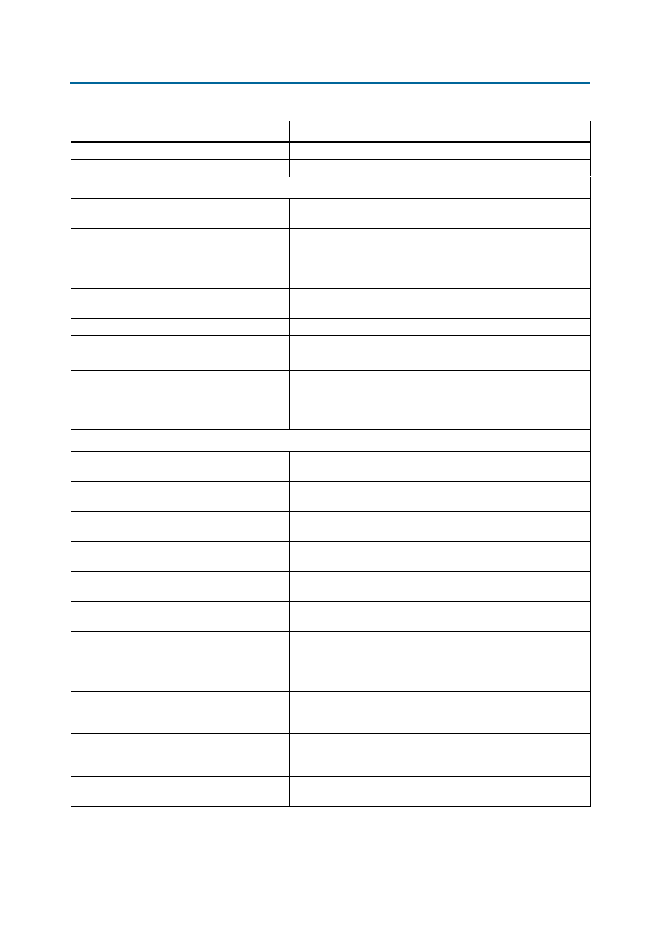
X3
100 M oscillator
100-MHz crystal oscillator for the MAX V CPLD System Controller.
J4, J5
Clock input SMAs
Drives LVDS-compatible clock inputs into the clock multiplexer buffer.
General User Input and Output
D6-D9, D17-D20,
D22-D31
FPGA1 user LEDs
Two sets of eight bi-color LEDs (green and red) for 16 user LEDs for
FPGA1. Illuminates when driven low.
D22-D25,
D28-D31
FPGA2 user LEDs
Two sets of eight bi-color LEDs (green and red) for 16 user LEDs for
FPGA2. Illuminates when driven low.
SW1
FPGA1 user DIP switch
Octal user DIP switch for FPGA1. When the switch is ON, a logic 0 is
selected.
SW3
FPGA2 user DIP switch
Octal user DIP switch for FPGA2. When the switch is ON, a logic 0 is
selected.
S3
MAX V reset push button
The default reset for the MAX V CPLD System Controller.
S7
FPGA1 CPU reset push button
The default reset for the FPGA1 logic.
S11
FPGA2 CPU reset push button
The default reset for the FPGA2 logic.
S4-S6
FPGA1 general user push
button
Three user push buttons for FPGA1. Driven low when pressed.
S8-S10
FPGA2 general user push
button
Three user push buttons for FPGA2. Driven low when pressed.
Memory Devices
U19, U57
DDR3A x32
512-MB DDR3 x64-bit data bus interfacing to FPGA1, consisting of
two x16-bit devices with a single address and command bus.
U30, U34, U72,
U80
DDR3B x64
1024-MB DDR3 x64-bit data bus interfacing to FPGA1, consisting of
four x16-bit devices with a single address and command bus.
U36, U81
DDR3C x32
512-MB DDR3 x64-bit data bus interfacing to FPGA1, consisting of
two x16-bit devices with a single address and command bus.
U21, U27, U58,
U68
DDR3D x64
1024-MB DDR3 x64-bit data bus interfacing to FPGA1, consisting of
four x16-bit devices with a single address and command bus.
U32, U75,
DDR3E x32
512-MB DDR3 x64-bit data bus interfacing to FPGA2, consisting of
two x16-bit devices with a single address and command bus.
U39, U43, U88,
U92
DDR3F x64
1024-MB DDR3 x64-bit data bus interfacing to FPGA2, consisting of
four x16-bit devices with a single address and command bus.
U33, U78
DDR3G x32
512-MB DDR3 x64-bit data bus interfacing to FPGA2, consisting of
two x16-bit devices with a single address and command bus.
U17, U24, U55,
U64
DDR3H x64
1024-MB DDR3 x64-bit data bus interfacing to FPGA2, consisting of
four x16-bit devices with a single address and command bus.
U12, U52, U41,
U90
QDRII+ x18 (interfaces A to D)
Four 4.5-MB QDRII+ SRAM interfaces with a 18-bit data bus for
FPGA1. The device has a separate 18-bit read and 18-bit write port with
DDR signalling at up to 533 MHz.
U22, U61, U40,
U89
QDRII+ x18 (interfaces E to H)
Four 4.5-MB QDRII+ SRAM interfaces with a 18-bit data bus for
FPGA2. The device has a separate 18-bit read and 18-bit write port with
DDR signalling at up to 533 MHz.
U4
MoSys x16
A 72-MB MoSys Bandwidth Engine IC SRAM with a 16-bit transceiver
data bus for FPGA1.
Table 2–1. Stratix V Advanced Systems Development Board Components (Part 3 of 4)
Board Reference
Type
Description