Altera Stratix V Advanced Systems Development Board User Manual
Page 66
2–56
Chapter 2: Board Components
Memory
Stratix V Advanced Systems Development Board
January 2014
Altera Corporation
Reference Manual
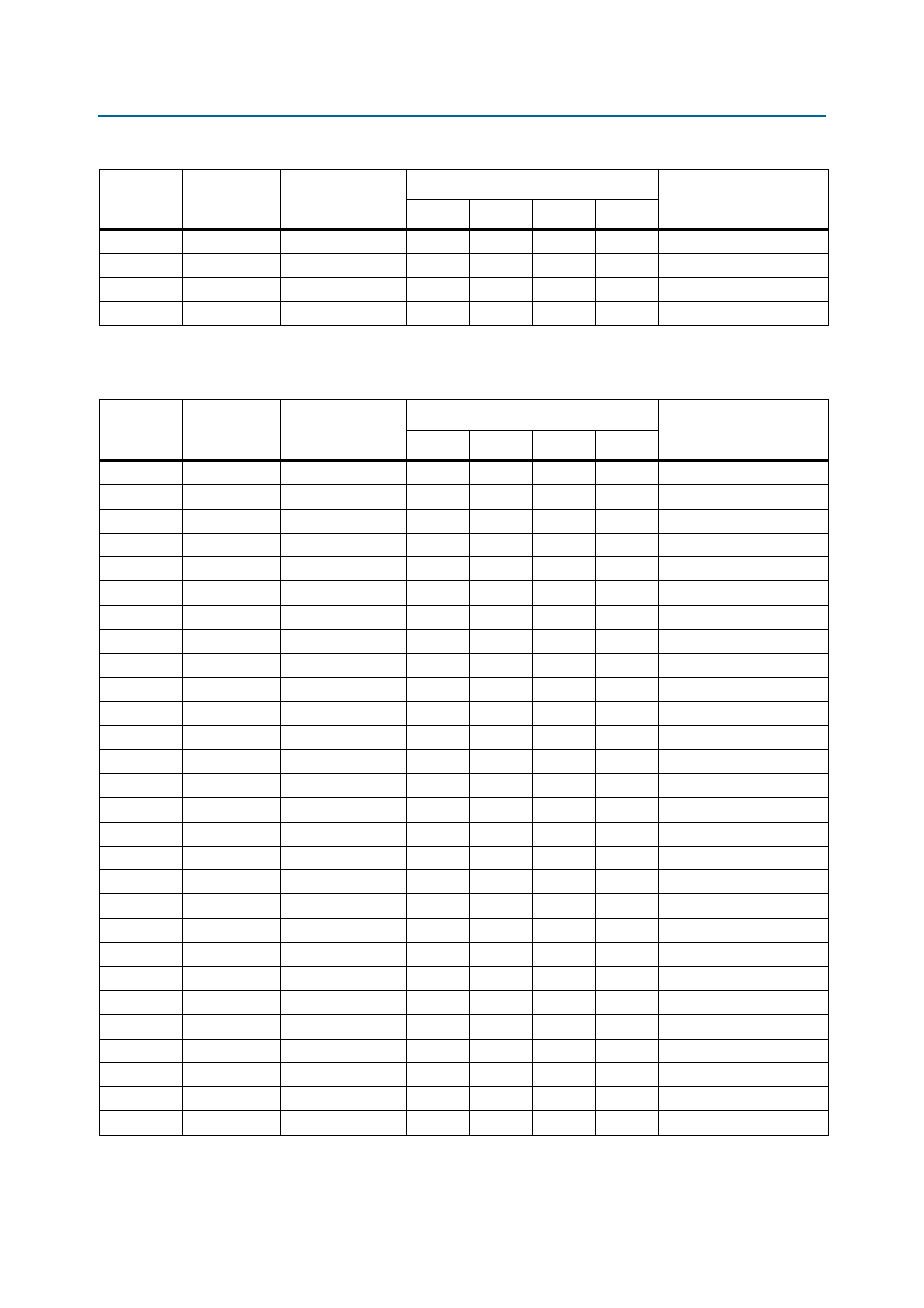
lists the QDRII+ pin assignments, signal names, and functions for FPGA2.
P3
Q17
1.5-V HSTL Class I
AH15
AW14
T29
E36
Read data bus
P6
QVLD
—
—
—
—
—
Read data valid (Unused)
A8
RPSN
1.5-V HSTL Class I
AV17
AH10
H30
U33
Read port select
A4
WPSN
1.5-V HSTL Class I
AR17
AJ10
N32
M38
Write port select
Table 2–25. FPGA1 QDRII+ Pin Assignments, Signal Names and Functions (Part 3 of 3)
Board
Reference
Schematic
Signal Name
I/O Standard
Stratix V GX FPGA1 Device Pin Number
Description
QDR2A
QDR2B
QDR2C
QDR2D
Table 2–26. FPGA2 QDRII+ Pin Assignments, Signal Names and Functions (Part 1 of 3)
Board
Reference
Schematic
Signal Name
I/O Standard
Stratix V GX FPGA Device Pin Number
Description
QDR2E
QDR2F
QDR2G
QDR2H
R9
A0
1.5-V HSTL Class I
BD19
AG12
J30
V34
Address bus
R8
A1
1.5-V HSTL Class I
BC19
AG11
M31
U35
Address bus
B4
A2
1.5-V HSTL Class I
AR17
AK12
A35
K34
Address bus
B8
A3
1.5-V HSTL Class I
AU16
AH10
C36
J36
Address bus
C5
A4
1.5-V HSTL Class I
AR18
AJ12
B35
K35
Address bus
C7
A5
1.5-V HSTL Class I
AT17
AJ11
B31
L36
Address bus
N5
A6
1.5-V HSTL Class I
AY16
AU10
D36
M36
Address bus
N6
A7
1.5-V HSTL Class I
BA16
AU9
C31
K37
Address bus
N7
A8
1.5-V HSTL Class I
BA18
AN12
C33
M38
Address bus
P4
A9
1.5-V HSTL Class I
AW16
AU11
P32
M37
Address bus
P5
A10
1.5-V HSTL Class I
AY18
AV10
C34
M33
Address bus
P7
A11
1.5-V HSTL Class I
BC17
AM13
D33
M39
Address bus
P8
A12
1.5-V HSTL Class I
BA19
AH12
E33
T35
Address bus
R3
A13
1.5-V HSTL Class I
AV17
AR13
T33
U32
Address bus
R4
A14
1.5-V HSTL Class I
AW17
AT12
T32
P33
Address bus
R5
A15
1.5-V HSTL Class I
AY19
AV11
N32
K36
Address bus
R7
A16
1.5-V HSTL Class I
BD17
AR12
H30
U33
Address bus
A9
A17
1.5-V HSTL Class I
AU17
AG9
D35
H36
Address bus
A3
A18
1.5-V HSTL Class I
AN17
AL12
R30
L35
Address bus
A10
A19
1.5-V HSTL Class I
AV16
AG10
B34
H37
Address bus (Unused)
B7
BWSN0
1.5-V HSTL Class I
AK17
AE13
Y27
G34
Write byte write select 0
A5
BWSN1
1.5-V HSTL Class I
AJ17
AD14
W28
F34
Write byte write select 1
A1
CQ_N
1.5-V HSTL Class I
AG16
AP15
T30
R36
Echo clock
A11
CQ_P
1.5-V HSTL Class I
AY15
AU12
K30
J37
Echo clock
P10
D0
1.5-V HSTL Class I
AV19
AW11
A32
V35
Write data bus
N11
D1
1.5-V HSTL Class I
AW19
AW10
F31
W34
Write data bus
M11
D2
1.5-V HSTL Class I
AU19
AE14
E32
T34
Write data bus
K10
D3
1.5-V HSTL Class I
AU18
AF11
D32
L33
Write data bus