Hsmc, Hsmc –37 – Altera Stratix V Advanced Systems Development Board User Manual
Page 47
Chapter 2: Board Components
2–37
Components and Interfaces
January 2014
Altera Corporation
Stratix V Advanced Systems Development Board
Reference Manual
HSMC
The development board contains a HSMC port that connects to the FPGA2 device.
This interface provides 8 channels of 12.5 Gbps-capable transceivers. The HSMC port
interface supports both single-ended and differential signaling.
f
For more information about the HSMC specification such as signaling standards,
signal integrity, compatible connectors, cabling solutions, and mechanical
information, refer
manual.
The HSMC connector has a total of 172 pins, including 120 signal pins, 39 power pins,
and 13 ground pins. The ground pins are located between two rows of signal and
power pins, acting both as a shield and a reference. The HSMC host connector is
based on the 0.5 mm-pitch QSH/QTH family of high-speed, board-to-board
connectors from Samtec. There are three banks in this connector. Bank 1 has every
third pin removed as done in the QSH-DP/QTH-DP series. Bank 2 and bank 3 have
all the pins populated as done in the QSH/QTH series.
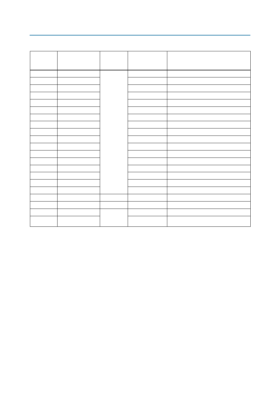
H7
FMC_LA_TX_P0
LVDS
(adjustable
VCCIO, 2.5 V
default)
F9
LVDS transmit or single-ended data bus
H10
FMC_LA_TX_P1
D11
LVDS transmit or single-ended data bus
D11
FMC_LA_TX_P2
K12
LVDS transmit or single-ended data bus
H13
FMC_LA_TX_P3
D10
LVDS transmit or single-ended data bus
D14
FMC_LA_TX_P4
K8
LVDS transmit or single-ended data bus
H16
FMC_LA_TX_P5
B7
LVDS transmit or single-ended data bus
D17
FMC_LA_TX_P6
K10
LVDS transmit or single-ended data bus
H19
FMC_LA_TX_P7
T10
LVDS transmit or single-ended data bus
D20
FMC_LA_TX_P8
M12
LVDS transmit or single-ended data bus
H22
FMC_LA_TX_P9
E12
LVDS transmit or single-ended data bus
H25
FMC_LA_TX_P10
H12
LVDS transmit or single-ended data bus
D23
FMC_LA_TX_P11
P8
LVDS transmit or single-ended data bus
H28
FMC_LA_TX_P12
U12
LVDS transmit or single-ended data bus
D26
FMC_LA_TX_P13
N11
LVDS transmit or single-ended data bus
H31
FMC_LA_TX_P14
P12
LVDS transmit or single-ended data bus
H34
FMC_LA_TX_P15
T13
LVDS transmit or single-ended data bus
H37
FMC_LA_TX_P16
U14
LVDS transmit or single-ended data bus
F1
FMC_M2C_PG
3.3-V CMOS
—
Power good input
H2
FMC_PRSNTN
2.5-V CMOS
BB9
FMC module present
C30
FMC_SCL
2.5-V CMOS
(adjustable
VCCIO)
A10
Management serial clock line
C31
FMC_SDA
B10
Management serial data line
Table 2–21. FMC Port Pin Assignments, Schematic Signal Names, and Functions (Part 5 of 5)
Board
Reference
(J8)
Schematic Signal
Name
I/O Standard
Stratix V GX FPGA1
Device Pin Number
Description