Development board block diagram, Handling the board – Altera Stratix V Advanced Systems Development Board User Manual
Page 9
Chapter 1: Overview
1–5
Development Board Block Diagram
January 2014
Altera Corporation
Stratix V Advanced Systems Development Board
Reference Manual
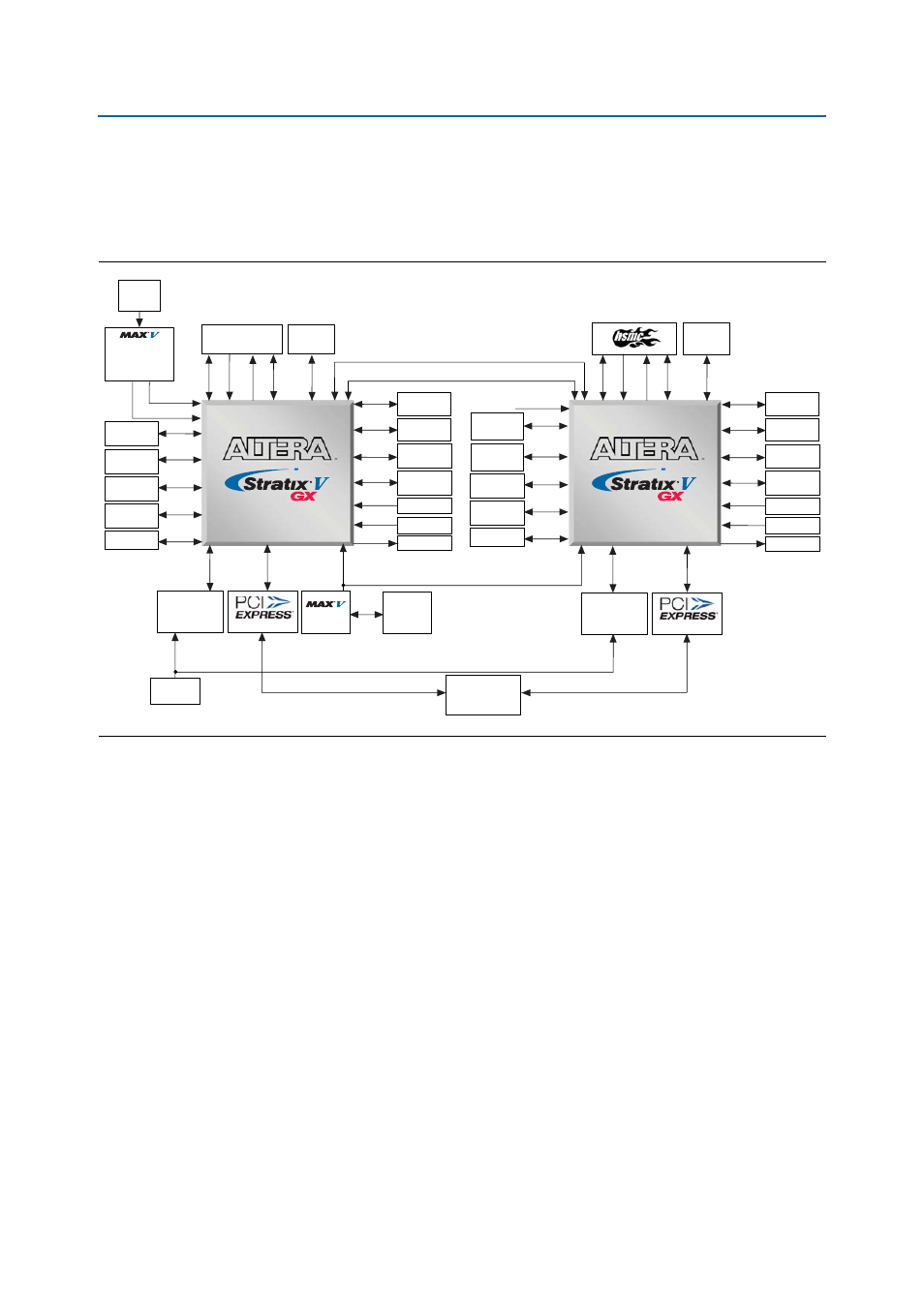
Development Board Block Diagram
shows the block diagram of the Stratix V Advanced Systems development
board.
Handling the Board
When handling the board, it is important to observe the following static discharge
precaution:
c
Without proper anti-static handling, the board can be damaged. Therefore, use
anti-static handling precautions when touching the board.
Figure 1–1. Stratix V Advanced Systems Development Board Block Diagram
5SGXEA7N2F45C2N
5SGXEA7N2F45C2N
On-Board
USB-Blaster II
and USB Interface
JTAG Chain
XVCR x8
Micro-USB
2.0
x19 USB Interface
LVDS/Single-Ended
FMC
MoSys
72-MB
1-T SRAM
XVCR x8
XVCR x16
MoSys
72-MB
1-T SRAM
XVCR x16
CLKOUT x3
x80
CLKIN x3
XVCR x8
CLKOUT x3
x80
CLKIN x3
512-MB
DDR3 (x32)
x32
JTAG Chain
512-MB
DDR3 (x32)
x32
1024-MB
DDR3 (x64)
x64
1024-MB
DDR3 (x64)
x64
4.5-MB
QDRII+
x18
4.5-MB
QDRII+
x18
x16
4.5-MB
QDRII+
x18
4.5-MB
QDRII+
x18
EPCQ
x4
512-MB
DDR3 (x32)
x32
1024-MB
DDR3 (x64)
x64
4.5-MB
QDRII+
x18
4.5-MB
QDRII+
x18
EPCQ
x4
x14
Push buttons
LEDs
x8
x3
x16
DIP Switches
512-MB
DDR3 (x32)
x32
1024-MB
DDR3 (x64)
x64
4.5-MB
QDRII+
x18
4.5-MB
QDRII+
x18
Push buttons
LEDs
x8
x3
x16
DIP Switches
Programmable
Oscillators
50 M, 125 M
x13
Programmable
Oscillators
50 M, 125 M
x8 Edge
x16 Edge
XVCR x8
x8 Edge
XVCR x8
CPLD
1-Gb
Flash
PLX PEX 8747
PCI Express Switch
x1 (LVDS)
x1 (LVDS)
XVCR x8
SMA Clock
Input
x8 Config
x8 Config
XVCR x8
LVDS x2, CMOS x12
CPLD